ISO5851: Fig. 6 of sllu218 "ISO5851 Evaluation Module" User's Guide related question,

Part Number: ISO5851

Tool/software:

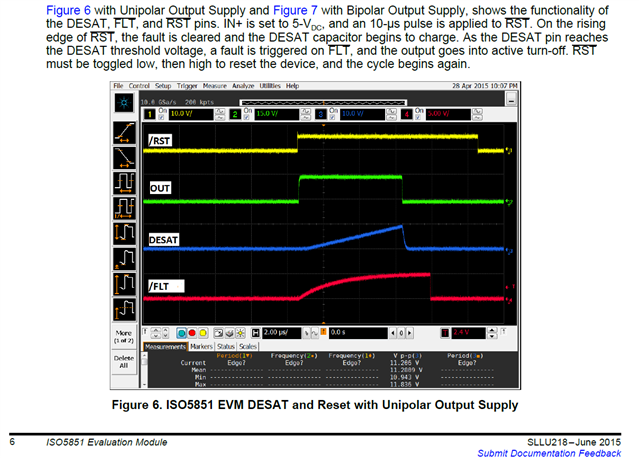
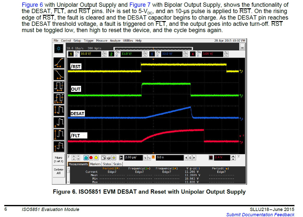
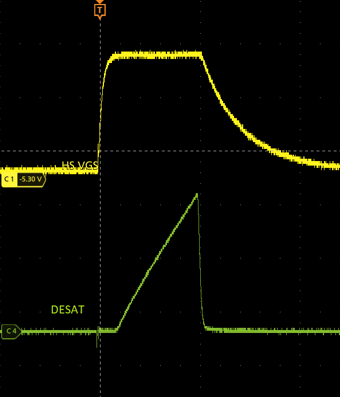
Fig. 6 of sllu218 "ISO5851 Evaluation Module" User's Guide (see below) did not explain how the DESAT waveforms are generated in this ISO5851 Evaluation Board & how it is implemented,

The related original detailed test procedures must have been kept in the related test report,   

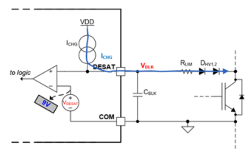
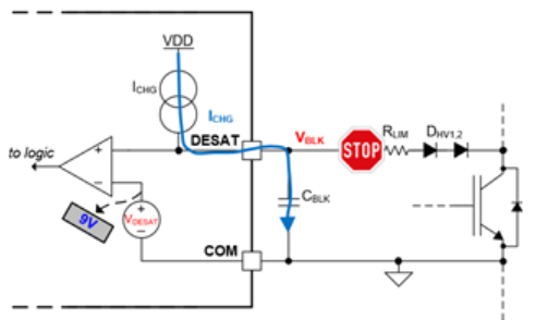
not sure if related DESAT related test component & schematic & steps can be shared with me, so we can know how it is implemented exactly to get the related Fig. 6 waveform?

this kind of information will be able to help customers who use this ISO5851 evaluation board to follow to do the related DESAT testing.

Thank you and look forward to hearing from TI when convenient. 

yenwu lo

  • Hello Yenwu,

    I would recommend taking a look at the following application note: Choosing Appropriate Protection Approach for IGBT and SiC Power Modules. Section 5 contains more information about DESAT Circuitry design.

    I hope this helps.

    Best regards,

    Muiz.

  • Thank you, Muiz, I am not asking about how to design this DESAT circuit, 

    I am asking about how the related waveform in FIG 6 is generated in the test bench using this physical evaluation board, for example, what equipment & steps performed which are used & executed to generate the related waveforms, is there inductor (how many Henries if used?) used in the physical test bench when doing this related DESAT test? the detailed steps to generate this waveform?

    Thank you & look forward to hearing from you when convenient. 

    yenwu lo

  • Hello Yenwu,

    The waveforms in the user guide were captured using only the EVM. There were no additional components added.

    The figures contained in the User Guide are example measurements using the EVM. The instructions for capturing the signals, along with the schematic, are provided within the User Guide. In this case, Figures 6 & 7 state in the caption, "IN+ is set to 5-VDC, and an 10-µs pulse is applied to RST" and Figure 5 shows the VCC2 & VEE2 values.

    I hope this helps.

    Best regards,

    Muiz Ishola.

  • Thank you, Muiz, I can read the captions associated with the FIG 6 without any questions, I understand also the FIG. 6 waveform are generated using the EVM board, 

    My question is, what the person who did this related test in the EVM board, actually did in the testing, so he is able to make the blue Dasat waveform to rise and then eventually trig the DESAT protection function as shown in FIG. 6 related waveform,

    This is because these steps, related setups & extra parts used to generate FIG. 6 related waveforms are not explained at all in the User Guide, I think it will be difficult for people who uses this EVM board to actually know & nothing to follow to generate those waveforms as shown in FIG. 6, 

    so, not sure if TI can share with customers the related information on how to perform the exact test steps to generate the FIG. 6 related waveforms.

    Look forward to hearing from you when convenient.

    Thank you.

    yenwu lo

  • Hi Yenwu, 

    As the user guide was published in 2015, the applications engineer who worked on this user guide is not with TI. I can offer some of my understanding here. 

    I believe in the testing, the collector terminal is left floating, which allows the DESAT node to charge up when output is high as there's no low-impedance path from the collector to the emitter. The nRST pin is toggled first to reset the device. After the nRST pin toggles, the DESAT voltage rises up as a result of the internal current source charging the capacitor. As DESAT voltage reaches the threshold, the nFLT and output goes low, and the device needs another reset before output can go high again. 

    Hope this helps, 

    Vivian

  • Thank you, Vivian, good day, I understand what you said above, 

    but my main question is what extra part & setup actually is used or involved & implemented in the Evaluation Board, which will cause the DESAT voltage to rise and reach the threshold, because the user guide does not mention it, 

    I think without using extra part & setup, the DESAT voltage will not be able to rise to the threshold automatically, 

    So, do you know what extra part or setup is used, to generate this the DESAT voltage to rise and reach the threshold?

    Thank you. 

    yenwu lo

  • Hi Yenwu, 

    No additional components are needed. The waveforms should happen when you don't populate any IGBT/FET onto the EVM and turns on the input. 

    When input is turned on, the DESAT charging current comes out of the DESAT pin. At this point, if there's an IGBT/FET connected, the output will turn the power switch on, resulting in a low-impedance path between the collector-emitter terminals, allowing the current to flow through IGBT/FET. 

    If there's no IGBT/FET connected, this low impedance path does not exist, resulting in the DESAT charging current flowing into the blanking capacitor, charging up the capacitor, and bringing up the DESAT voltage

    I've done some similar experiment before. By simply turning on the output and leaving the collector terminal floating, the DESAT voltage rises up. 

    Hope this helps, 

    Vivian

  • Thank you very much, Vivian, your approach can be used to determine the DESAT trig voltage, & check DESAT function actually working or not.. 

    But without a real IGBT & some extra setup in the EVM board, it might be not easy to demonstrate a real DESAT application example.

    However, you already have answered my question, I have no more questions on this at this time, please help to close this case. Thank you again. 

    yenwu lo