UCC28951-Q1: Continuing search for cause of outsized surged in primary current every switching cycle

Part Number: UCC28951-Q1
Other Parts Discussed in Thread: UCC28951, UCC28950, UCC28950EVM-442

Tool/software:

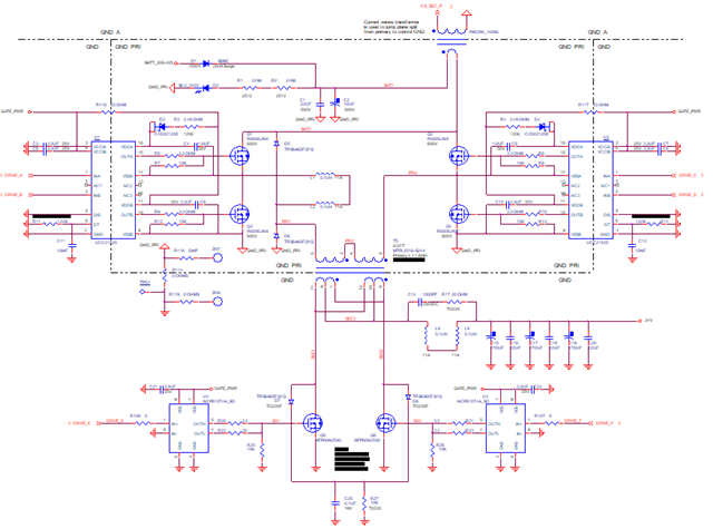
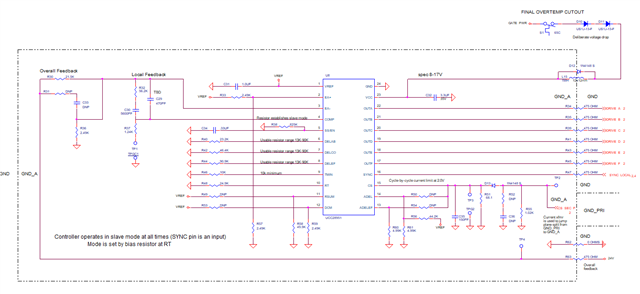
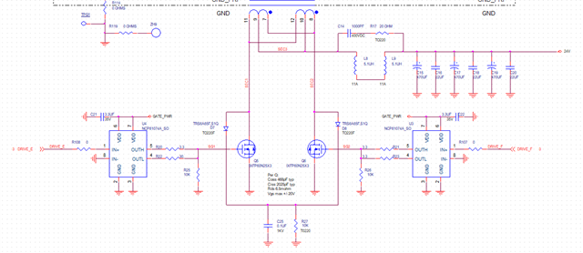
Suspecting improper connections or timing of secondary FET gates as the cause of large current surges that overpower reflected secondary current ramps, I have inspected the connections of all gate drivers (I believe they're OK)  and have used SLUC222D to recalculate resistors at DELAB, DELCD, and DELEF.  On the CS-feedback side, I have ADELEF connected to ground through 4.99K,  and have ADEL connected the same but with 44.2K also connected to VREF. While debugging this destructive current I am running at 25% load and relatively low input power voltage to avoid the need for current scaling. (At full power the bridge FETs only last a few seconds.)

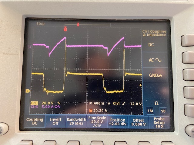
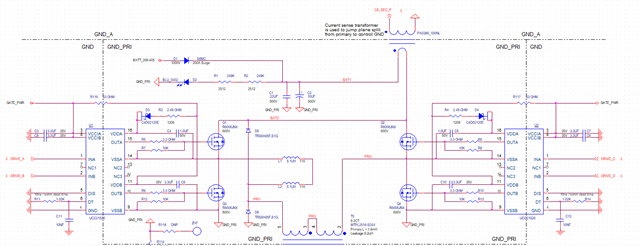
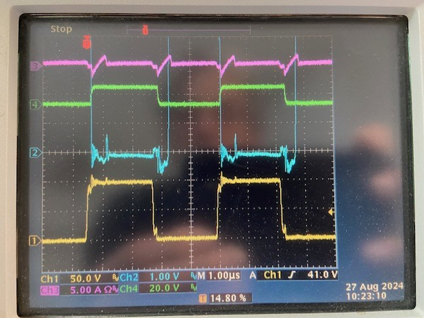
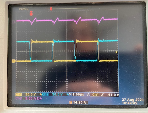
The photo I sent in an earlier post had a misleading trace (magenta,second from top) which I had incorrectly identified as the center tap of the secondary, which it can't have been. But at least it served as an invitation to sketch in what the secondary center tap should have looked like.  All photos below are from the delay-adjusted circuit described above.  The first photo has just two traces: The upper trace is the power input current, taken at the top of the bridge with a current probe.  It still shows the unexpected surge as well as the expected reflected-secondary current ramp.  The lower trace is in fact the secondary center tap. Note that the unexpected surge consumes about half the dead time between secondary power pulses and ends precisely at the beginning of the power pulse.  

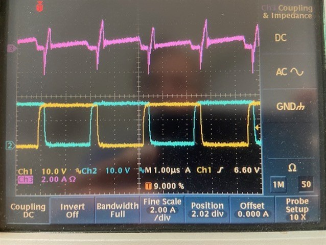
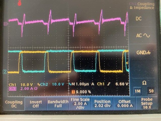
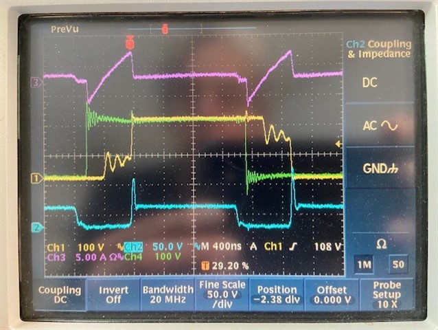
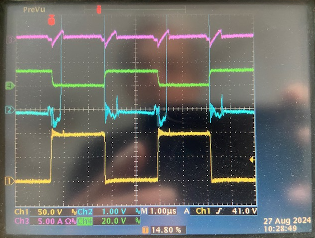
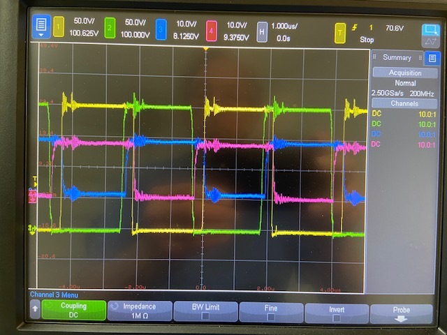
The photo below shows the two ends of the bridge (yellow and green, larger waveforms), and the two secondary gates (blue and magenta, smaller waveforms).  Note that the gates signals overlap their corresponding primary signal times, and nearly overlap each other. Is this timing correct?

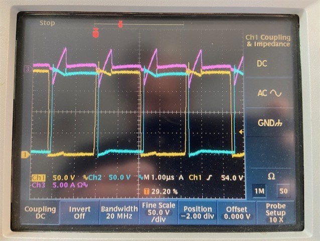
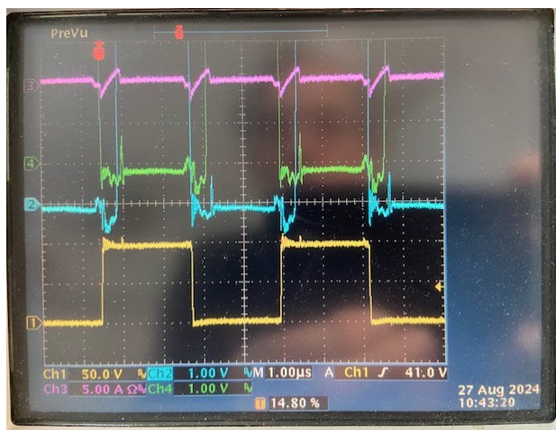
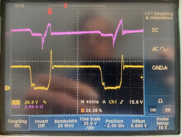
The last photo shows the primary current and the secondary gates.  Here it looks like the two secondary gates do overlap.  Note the alignment between the current surges and the apparently-overlapping gate signals.  Is there a relation between these beyond coincidence?  I was surprised to find this overlap. I'm using NCP81074A gate drivers. These have separate rise and fall outputs.  Right now the gate resistors are the same and quite small (3.3 ohms). Should I perhaps make the rise resistors substantially larger to try to get some separation between the secondary FET on-times?

  • Hello,


    This last image explains where the negative current is coming from on the primary.  During the freewheeling of the design when both SRs on the current in the output inductor is going negative.  When the design comes out freewheeling the CT shows this negative current.    I would set the DCM comparator of the UCC28951 to turn off the SR driver before the inductor goes into critical conduction.  This will prevent the negative current and hopefully will remove your issue. 


    Regards,

  • Thanks! I will go study up on the DCM comparator.  Meanwhile, I had begun study of another unit that has no SR drive at all.  Gate pulses are entirely turned off. (I frankly don't know why they're off (the E,F drive outputs of the chip are zero), but I decided to take advantage of the situation by studying the primary current when SR conduction is not an issue at all because it never happens. Remarkably, the primary current surge persists!  (I'm thinking this test even supersedes the one you've just suggested, but I will still study it.)

    The first photo shows primary current in the upper trace, secondary center tap in the lower trace:

    Note that the unexpected current ramp ends at the beginning of the secondary power cycle.

    The second photo shows primary current, as well as the two bridge signals:

    Note that the unexpected current ramp begins at the start of the primary power cycle (where the left side moves opposite the right side).

    Bear in mind that the only secondary conduction is now through the SR FET body diodes, since there is no gate drive. So SR timing is not in play at all.  

    Third photo shows the bridge left side and the shim-primary junction rather than bridge left and right sides, and adds the secondary center tap:

    Here it is clear that the unexpected primary current ramp occurs coincident with the time during which the primary voltage change is dropped entirely across the sum of the shim and the leakage inductance.  Given that these secondary FETs are not being turned on at all (I've checked their gates for a third time now!), what can be happening to cause these primary current surges that (I presume) do not occur in a working system?

    NOTE: I see that SLUC222D says the transformer alone has more leakage inductance that this circuit needs, and I've added twice that again with the shim.  Could all of this be a case of too much shim?

    Would it be helpful for me to share the full schematic?  I don't want to publish it, but if there's another way to directly share I could do that.

  • Hello,


    Your inquiry will be review in the order it was received.


    Regards,

  • Hello,


    I think there may be an issue of how you are using the current sense transformer.  Your current out of the CT should resemble the current in the primary of your transformer and it does not.  I would double check your CT placement and setup.  The following link will bring you to an application note on how to to design with the UCC28950 and has information on how to place the CT and set it up.  I think this information should help you resolve the issue. https://www.ti.com/lit/pdf/slua560


    Regards,

  • The current measurements shown are from a current loop directly in the feed to both sides of the primary FET bridge.  This current loop is in place of the current transformer which was removed to eliminate any errors it might cause from the measurements. A DC current probe measures the loop current and displays it on the oscilloscope.  There is no current-sense transformer in the circuit at this time. Also, I don't believe I've presented any traces of primary current. I have presented voltage traces that can be used to infer the primary differential voltage. (This would be the shim-junction trace of the last screen shot minus the right-side bridge voltage from the second screen shot.)

  • Hello,


    Originally you reported this waveform as coming out of your CT.  If you used a current loop and the CT signal looks the same you should put the CT back in circuit.

    The input current to the H Bridge does not look correct.  It should be similar in shape to what is in the primary of the transformer current.  It also should not be going negative.  Have you checked this?

    There is something in your design that is off.  I am not quite sure what it is.  Did you check the design versus what was recommended in application note slua560?  https://www.ti.com/lit/pdf/slua560 That should point you in the direction of what is causing the H Bridge input current to be off.


    Regards,

  • Hello,


    If you can’t share the schematic on the e2e and need direct customer support you will need to get in touch with your local Texas Instruments field application engineer for support.


    I do think there is something different in your design.  The other option might be to order the 600 W evaluation module, UCC28950EVM-442, to evaluate and compare to your design.  The UCC28950 is identical to the UCC28951 except the UCC28951 was designed to operate at duty cycles greater than 90%.  The specifications and pinout are identical.  The following link will get you to the UCC28950 evaluate module if you are interested in ordering it for evaluation.

    https://www.ti.com/lit/pdf/SLUU421


    Regards,


    Related thread information on a second thread.  Added for additional information for e2e readers.

     UCC28951-Q1: Continuing search for cause of outsized surged in primary current every switching cycle 

  • It will take two B-size sheets to convey the critical parts of the design. Should I drop screen grabs of these full sheets onto this forum for inspection?

  • Hello,


    I will review the schematics if you provide them.


    Regards,

  • The next two images are only screen grabs from an HD screen; they may not have sufficient resolution to be useful.  I may have access to a 4K screen to grab from tomorrow if these can't be read.

  • Here's the first page in halves for better readability:

  • Hello,


    I have received your inquiry and will have recommendations for you tommorow.


    Regards,

  • Hello,


    I reviewed your schematic and cannot see how this negative current is developed during the free-wheeling period.  This waveform was taken from the input of the H bridge with a current loop according to your notes.  This is during the free-wheeling period.  FETs QA and QC are on at the same time or FETs QB and QD are on at the same time.  This means the transformer primary and shim inductors are shorted across the FETs  So where is this negative current coming from.  It also changes direction right be the design comes out of freewheeling.  


    I am wondering if this current is from the clamp diodes.  Just as an experiment could you short out L1 and L2 and see if the current waveform changes?

    That would verify if the current is indeed comming from the clamp diodes.


    Regards,

  • I've been thinking along these lines, and did an experiment a while back that shorted L1 and L2.  The result of that is to remove the negative-current first half of the input current aberration.  The last half (form zero to several amps) remains. I've also tried replacing L1,L2 with an additional current transformer to monitor current of the primary.  That waveform looks just like the input current waveform, except for the expected alternate-half-cycle inversions since it's inside the bridge.

    Those experiments left the question of where this current suddenly goes at the end of the large ramp - and in the case where L1,L2 are still in the circuit, where it suddenly comes from when it appears as a large negative current. I'm working a theory on that, but new measurements I've taken to confirm or debunk it are adding to the confusion so far.  Haven't had much time to think them through yet.

    Here's my theory: The place this large current disappears to is into the secondary-side snubber. You can see the large pulse in the secondary center tap screen grabs above.  I've compared the calculated energy storage of the leakage + shim current to that of the snubber capacitor voltage and found comparable values. So I'm fairly sure that's where it goes. 

    The next question is where the current comes from.  In the circuit version with shorted shim inductor (the version that starts at zero current rather than a large negative current), this could come from current built up during reverse recovery of the secondary FET body diodes. Bear in mind, this aberrant primary current appears whether or not the secondary gates are driven.  In the case of no secondary FET gate drive, all of the output load current will be conducted through these body diodes alone. When the bridge polarity changes, the voltage across the body diodes will be close to zero until the reverse recovery time has elapsed. This will cause a rapid current ramp in the leakage inductance.  I have calculated the expected di/dt and find it matches the magnitude of the aberrant primary current ramp perfectly.

    Going back to the circuit version that includes the shim inductor (L1,L2), the next question is where the large negative current suddenly comes from. My theory here is a little more hazy, but I think it makes some sense.  And here's where the clamp diodes come in. Assuming again that we start with a saturated body diode and reversing the bridge, the secondary will stay near zero until the end of the diode reverse recovery. At that point, the secondary and primary transformer voltages will fly up, dumping leakage inductor energy into the secondary snubber.  But the junction of the shim inductor and the leakage inductance (the transformer primary) can't go beyond the positive rail because that junction is clamped by the SiC clamp diode.  So the energy stored in the shim inductor is trapped in the inductor by the short formed by clamp diode and high-side bridge FET. When the bridge next switches polarity, that current (still stuck at close the value at the end of the reverse-recovery event, will appear at the input with inverted polarity. 

    I think this may all make sense when the output FETs aren't driven. But when they are, the FET conduction should prevent charge buildup in the body diodes, so there should be no reverse recovery time to cause this large current buildup.  But it still happens. I'm trying to investigate this now.  I'm working that from two angles. 

    First, I've replaced the secondary FETs with Schottky diodes on one unit. That's not a good solution because it will cause another 5% or so power loss on my 24V supply due to voltage drop. But (excepting increased capacitance), the reverse recovery event should not occur.  I have yet to test that version but plan to get to it soon.

    Second,I've taken high-sensitivity oscilloscope measurements of the secondary FET drains (on a unit that does drive the gates!), to see if the voltage indicates FETs preventing diode conduction (~ 0.1V drop) or silicon diodes conducting (~1V drop).  The answer seems to be some of each. Maybe secondary FET timing is the issue. It looks like perhaps the 

    I will post screen shots of this shortly, along with results of running with Schottky diodes in place of secondary FETs.

  • Hello,


    Thanks for the update.


    Regards,

  • Here are screen shots of the secondary FET drains and related signals mentioned above.  This is of course the assembly version that has FETs, not Schottky diodes.

    Above: input current probe, Q5G, Q5D,Q2S.  Here we see that the secondary FET Q5 is turned on for the full time the primary side is energized. And the drain voltages indicate that the body diode is begin kept out of conduction, with the possible exception of the last  few tens of nanoseconds.  Even here, drain voltage barely touches 0.6V; it seems unlikely that a silicon diode will be hard to reverse after that.  And yet the high primary current surges persist.  This seems to argue against the excess current being built up during the reverse recovery time of the body diodes.

    Above: Same as previous except showing opposite bridge signal.  Timing is slightly different due to phase shift across bridge; seems identical otherwise. No smoking gun here, it seems.

    Above; substituting the other secondary drain signal for the gate signal. Again, seems to show little opportunity for body diode to saturate hard enough to need a lot of charge transfer to reverse.

    Above; showing the symmetry of the two bridge sides.  Seems like I'm following another dead end. Nothing looks like it should be dumping energy into the leakage inductance 

    NEXT UP: Will test the version that substitutes Schottky diodes for secondary FETs.