This thread has been locked.

If you have a related question, please click the "Ask a related question" button in the top right corner. The newly created question will be automatically linked to this question.

TPS63070: Solder failures: Solder wicking into vias on pads

Part Number: TPS63070


Tool/software:

Hi E2E community,

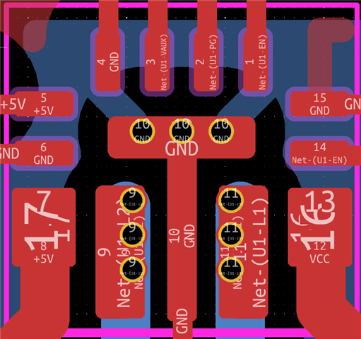
I've built some PCBs with TPS630701, designing the pcb footprint as it was recommended in technical references. However, it seems like during reflow solder wicks into vias on pad 9-10-11 sometime leaving insufficient solder which leads to failures right after the reflow process or after being subject to minimal mechanical impact.

What sort of solution would you recommend to avoid failures? (Ideally solutions which won't make the PCB more expensive :)

Many thanks,

Ersin

  • Hello Ersin,

    thank you for using E2E.

    Did you plug the vias on the bottom side of the PCB?

    Best Regards,
    Johannes

  • Hi Johannes,

    Yes, they are connected to bottom layer. On the bottom side they are tented.

    Thanks,

    Ersin

  • Hello Ersin,

    For boards that are not produced yet, I recommend filling the vias with some material another possibility is reducing the size of the vias until no solder flows in and increasing the numbers of the vias for heat dissipation.

    Best regards,
    Brigitte

  • Updates,

    I have removed the vias under the pad and problem seems to be solved. 


    To conclude, the main problem was over engineering in the evaluation board design and the layout example in the datasheet. This was a great learning exercise: good engineering is keeping things simple, and remove anything which doesn't need to be there to begin with.

    Also, I have spoken to some experienced peers and they agree that not all the TI evaluation board designs are good references. Perhaps they should not be used in the datasheet to avoid unnecessary complications.

    Thanks,

    Ersin