Hai TI team, I would like to get insight about the clamp circuit connection when driving 2 mosfets in parallel. I have read the forums and in there it is mentioned to use a pnp transistor with clamp pin and then connecting to the gate,the resistor value(10ohm) given on the clamp pin and before the transistor(100ohm) can be used for UCC21710 as well? Also, if iam using current booster, the turn on and turn off gate resistors are placed after or before the NPN-PNP transistor for the parallel connection? how is R8 choosen ?

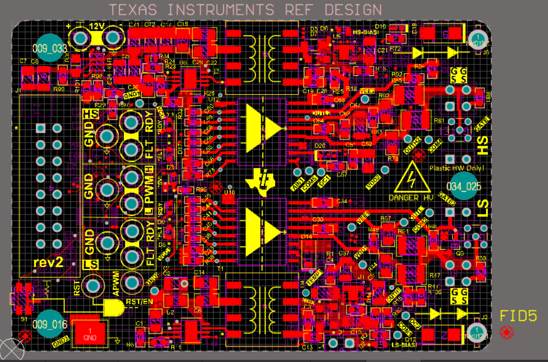
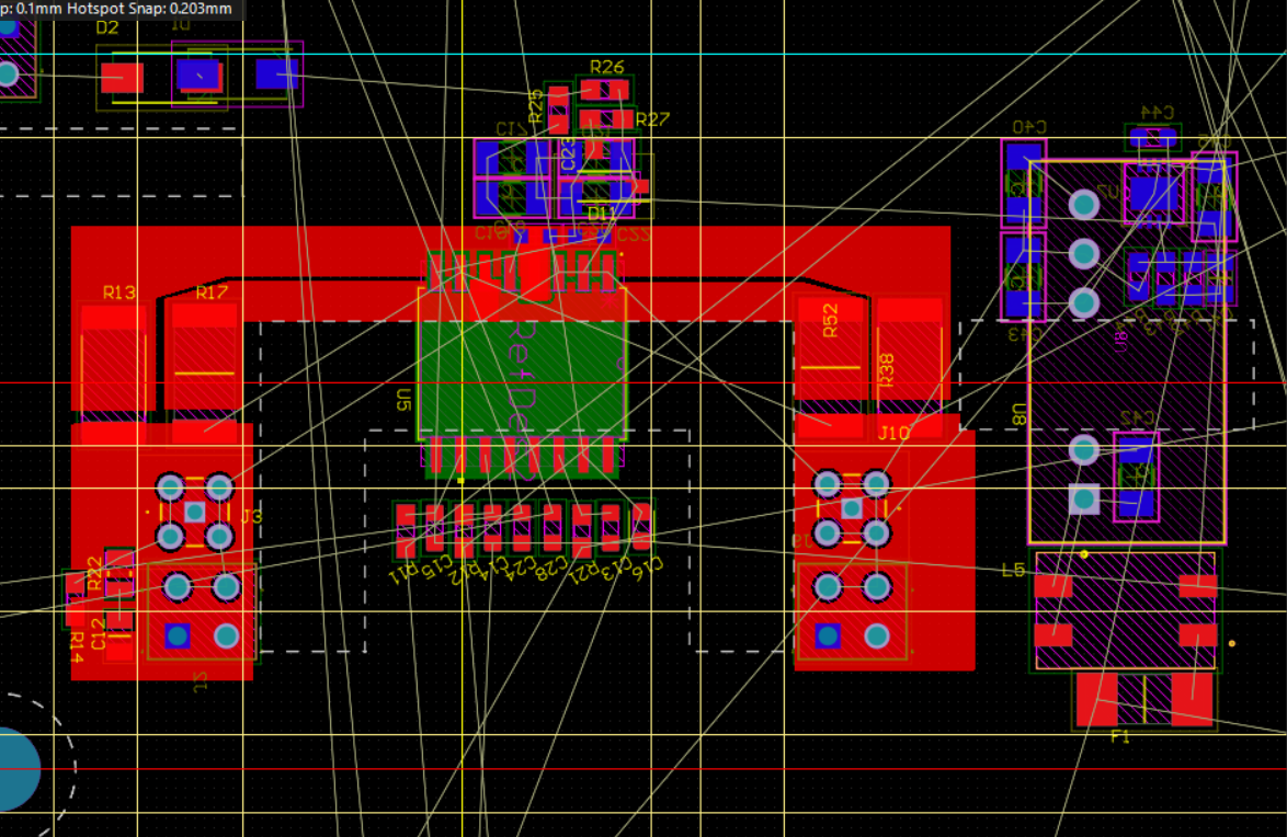
Furthermore , while doing the layout, I know an isolation barrier (Clearance) is necessary between primary and secondary part of the IC but is it necessary with the DC/DC converter also? in the reference evalboard design TI has also done the same (making it a single line)but when it comes to paralleling connecting from same driver IC to 2 gate of mosfets its getting harder for layout with the isolation barrier for DC/DC converter, could you please check the image if i could break the isolation barrier for DC /DC and pour it like this ? (iam using Vincotech's internally paralleled halfbridge powermodule 30-EP232PB004ME01-PR09F07T )
Kind regards
Hariprasad