Part Number: TPS65987DDK
Hi
I've been attempting to use the TI application customization GUI tool to enter DP alt mode. I understand this part is now NRND however it is being used in an existing design which is being modified to support alt modes.
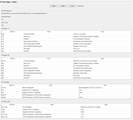
I'm able to enter a PD power contract successfully and can see that alt mode details are available, however if I manually go to the configuration registers whilst in debug mode and change the DFPD receptacle pin assignment in register (0x51) and write that data, this doesn't seem to change the values I read back from the DP SID Status (0x58) in debug registers after reading.
I'm running in APP mode and connected over I2C. The device I'm connecting to supports DP Alt mode. I've taken a couple of screen shots and attached the related project.
I'd welcome your suggestions on items to adjust in the design to successfully enter alt mode.
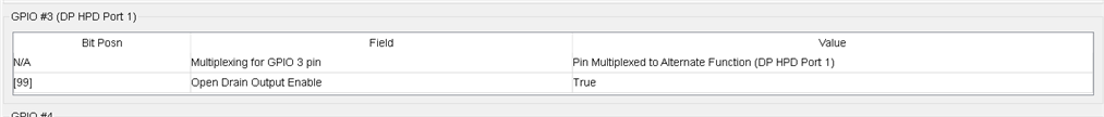
A further question, when using GPIO3 for HPD signalling is an external pullup resistor required or is this integral to the IO?
Regards
Malcolm
TI_TPS65987DDK_FPGA_8_DP_DFP_ONLY_HPD.pjt