This thread has been locked.

If you have a related question, please click the "Ask a related question" button in the top right corner. The newly created question will be automatically linked to this question.

TPS63700 does not always come up

Other Parts Discussed in Thread: TPS63700

Hello,

The customer submitted this case to support@ti.com Service Request # 1-756938091

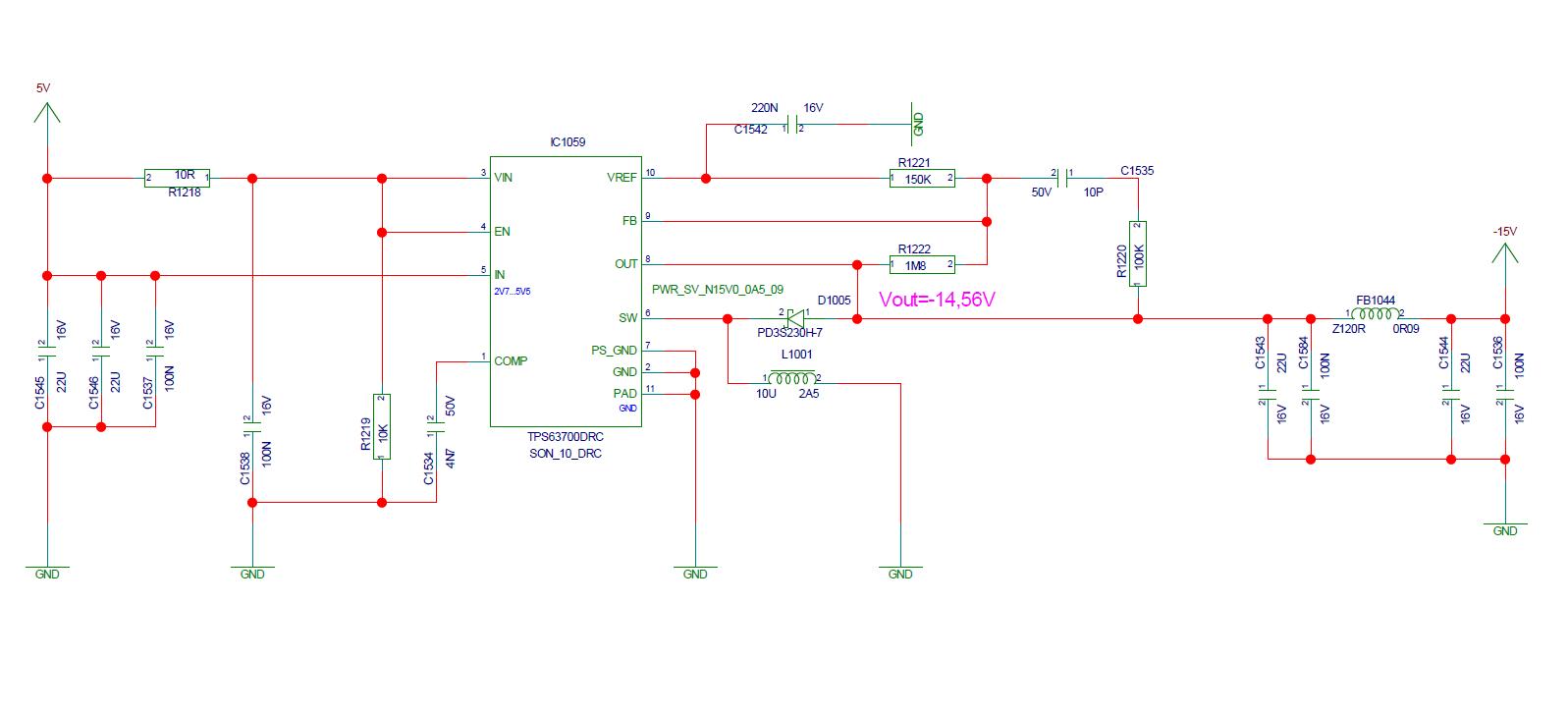
The problem that we are seeing involves a -5V supply module (See attachment).  The TPS63700 (U1) creates -6.2V which is then followed by a linear regulator to create a clean -5V supply.  Using a bench supply to power the module, we have no problems.  In the final application, the power supply has a very sharp turn-on profile, and we have problems.


During some power-ups, this supply doesn’t come on at start up (Maybe 25% of the time, but most likely when powered off for 30 sec or more).  At these times we have  5V at the input and +0.6 at the output. 


 We started adjusting the values of L2, The charging inductor.  Taking the value down to 2.2 seems to make things worse, except at -40 C, when that appeared to be a good value.  Changing the value of L2 up to 10uH looks to have fixed the problem in all situations, But we are very unsure of the reasons behind what seems to be the fix.


  • I did not see an attachment.

    Is the output voltage at ground or is it already being pulled below ground by some other rail?  We have recently found that the IC will not reliably start up if the output is "pre-biased" to a voltage below ground.

    If not pre-biased, then the most likely cause is switching noise getting into the IC through the FB and OUT pins.  All inverting "buck-boost" converters have more switching noise than other topologies.  The TPS63700 current limit circuit is very sensitive to this switching noise and will sometimes false trip, thereby preventing the output from reaching its regulation voltage. Optimizing the board layout to minimize switching noise will eliminate this problem.   I wrote an appnote to explain how to reduce switching noise in an inverting buck-boost converter:  http://www.ti.com/litv/pdf/slva219a

    As you have seen, increasing the inductor, which reduces inductor current ripple and therefore output voltage ripple (part of the switching noise), may eliminate the problem as well. However, improved layout is the best solution.

  • Jeff,

    Thank you. I am attaching the schematic. When TPS63700 does not start up, the output sits at +0.6V.

     2235.TPS63700.pdf

  • After seeing the schematic, I think your issue also includes VREF collapsing because R2 is too small.  VREF can only reliably provide 1.213V with a 10uA or smaller load, as shown in the spec table.  R2 of 90.9k pulls 13.3uA from VREF.  I recommend increasing R2 to reduce the load on VREF below 10uA. 

    If C3 and C5 and the 10uF caps on the input and output are as close possible to the IC, then the only other issue is the 10uF output capacitors themselves.  On the EVM, I used 4x4.7uF ceramic capacitors because the frequency response of larger capacitors, at the time the EVM was development, showed a resonance point below the IC's 1.5MHz switching frequency.  Therefore, 10uF+ ceramic capacitors would not behave as capacitors at the IC's switching frequency.  Also, ceramic capacitors must be derated based on their dc bias.  For example, if you selected 6.3V rated 10uF capacitors for the output, they will retain than 1/3 of their 10uF capacitance with -6V across them.  So, you might check the capacitance datasheet to determine the actual value of capacitance at the rated output voltage and switching frequency. 

  • Jeff - Thank you very much for your comments.

    Alex

  • Jeff,

    The customer provided some plots and some  additional information (see attached files). Please advise.

    3542.PCB1507291_A.pdf


    Normally L3 is a 4.7µH inductor I have included plots of the inductor current during steady state operation with a 111mA load and during start-up.  The power supply appears to operate in a continuous conduction mode at steady state.  I change the inductor to a 2.2µH to force it to operate in a discontinuous mode to look for instability. While using a 2.2µH inductor I was able to recreate the problem and have included the plots.


    • The failure mode appears to be unstable at the start.  The inductor current increase until about 995 mA which is the current limit for the chip.  It then locks-up but the Vref is still present.


    • I was concern that I am using pin 7 PS-GND to decouple the output diode D1, in the functional block diagram it goes to the control logic.  Could this contribute to the lock-up, it appear to be deliberately avoided in the Evaluation Board layout.


    I am working on a change to the layout because of a unrelated pin issue and I am considering the following changes (layout attached).


    • Change the R2 & R3 to limit the Current for the Vref to < 10µA
    • Changing the location of C5 to decouple to the lug ground similar to the Evaluation App Note.
    • I am also removing the ground under L3 in the event that it is capacitive coupling noise to ground.


     4338.4.4uH inductor waveforms vs 2.2uH.docx

  • Yes, PS_GND should not carry switching currents and only be tied to GND at one single point, usually at PowerPad.  So, changing the layout to match the EVM and app note should fix your customer's problem.

  • Hallo Jeff,

    we've got the same problem in our design. TPS63700.

    If an under voltage condition appears, the device turns off and sometimes it doesn’t come up. The same behaviour at power up process. My collegues has tested an evalboard with TPS63700 and has determined the same behaviour. I have attached a picture with our schematic. Unfortunately I cannot find such a small device.

    Do you know some solutioins for this problem?

     PS: Strange, I'm not able to attach file here.

    Best Regards


    Vitali Lach  


  • To attach a file, simply use a paper clip button when writing your post.

    Could you post a waveform (taken on the EVM) of Vin, SW and Vout when the device turns off?  What changes did you make to the EVM to obtain this waveform?

  • Hi Chris,


    Unfortunately I’m working currently in another project. I will try to find the time to test this device.

    Best Regards