This thread has been locked.

If you have a related question, please click the "Ask a related question" button in the top right corner. The newly created question will be automatically linked to this question.

TPS63060 exhibits strange results when the input is 3.3V and the output is 3.3v

Other Parts Discussed in Thread: TPS63060

Hello,

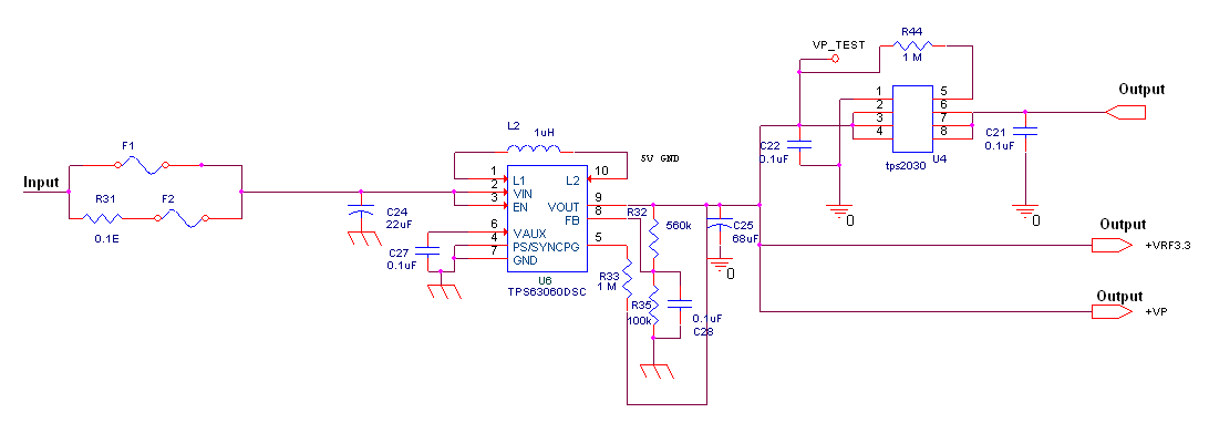
My customer is evaluating TPS63060 using EVM. They sweep the output voltage using external DAC and a resistor (see attached schematic). 

They developed transfer curves (three plots - see attached EXCEL file with three tabs). The Y-Axis is the output voltage and the X-Axis of the transfer curves is the MTR_PWR_ADJ signal in the schematic.

First plot shows Vin of 4V no load and it looks great.

The second plot Vin=4V, with 15ohm load and the output looks reasonable other than when the output is around 3.5V (seems like some sort of a hysteresis).

The third plot shows Vin=3.3V, with 15ohm load and the output "wobbles" in the middle. The transfer function is not monotonic.

Is the circuit going unstable? Different compensation required?

Thank you,

Alex

5127.mtr_pwr.pdf

5861.mtr_xfer.xls


  • When the TPS63060 is transitioning between buck and boost modes, there will more output ripple as the converter bucks for a few cycles and boosts for a few cycles. There is no hysteresis, the transition between buck and boost will happen automatically and frequently as VIN and VOUT near each other. You can look at the voltage of pins L1 and L2 with an oscilloscope to see the transition; L1 and L2 should match the plots in the EVM user's guide (see figure 4). Since you have power save mode enabled, the converter will also automatically transition between PWM mode and PFM mode. In PFM mode, at light load currents, the output voltage will be approximately 2.5% above the PWM set point. You will see bursts of switch cycles on L1 in buck mode and on L2 in boost mode. Also, please verify that your layout matches that of the EVM.

  • Is there any solution to avoid this wobbling as it is too high in my case. I needed 3.3V as output constant max 3.5V constant. But this fluctuation is driving me crazy. My input  varies from 2.5V - 9V Max . Under no load condition the wobbling is too high after i cross 5V it reduces to my desired value. What am i suppose to do to avoid this wobbling at input voltage3.0V to 4.0V.

  • Yes, you can add more output capacitance or operate in PWM mode to reduce the ripple.  Note that 'too high' may mean something different for different applications.

  • Hi

    As per your suggestion I connected a higher capacitor ( Increased from 66uF to 100 uF ). But still I am facing the problem in boost mode where the supply is varying from 2.6V to 4.2V which is not recommended in my application and could turn hazardous to the devices connected to it. The input applied to the IC was a battery supply (4.08V) and only with a load of 27 Ohms load was connected . Also the IC gets heated up.

    The noise generated from the current limiter is also too high.

    I have attached my design along with this please do the concern

  • I recommend ordering the EVM and doing your testing on it.  You likely have a board layout issue.

  • Thanks for your support.

    The problem got solved today by replacing  the 0.1uF capacitor with 10pF capacitor. which was the mistake i did during the realization of this circuit.

    Regards

    Heramban

  • 6746.TPS63060DSC.docx

    Hi   

    I have attached an document along with this mail where it contains all the readings which I observed while testing the IC. It has been connected to an current limiter TPS 2030. Please verify the document and confirm weather the device would function by providing that amount of ripple and spikes.

    I also would like to inform that our requirement cannot provide large current to support huge capacitors as well reduce the ripple around 100mV peak - peak.

  • Your question is not clear.  Only you can determine if the output of the TPS63060 through your current limit switch is sufficient for your application.

  • Hi 

    I have designed an multilayer (6 Layer) PCB for this TPS63060 IC where I have used a common ground plane which interconnects the control ground and the power ground pins of the IC via PTH. Is this advisable or is there any remedy to done.

  • The grounds need to be connected and under the IC on the thermal pad is the recommended place to do this.