This thread has been locked.

If you have a related question, please click the "Ask a related question" button in the top right corner. The newly created question will be automatically linked to this question.

TPS40211 - SEPIC

Other Parts Discussed in Thread: TPS40211, TPS40210

Hello:

The TPS40211 datasheet has design equations and a step-by-step design procedure for a boost regulator circuit.

Does something like this exist for designing a SEPIC regulator with this device?

Any feedback or input is welcomed and appreciated!

Thanks again!

Paul

  • Hi Paul,

      Yes, we have a SEPIC design for the TPS40211.  It is available here: http://www.ti.com/litv/pdf/slva442 .

    As well an AAJ article: http://www.ti.com/lit/an/slyt302/slyt302.pdf .

    And a PMP4729 design: http://www.ti.com/tool/pmp4729 .

    This design is referenced directly on the TPS40211 Product Folder page: http://www.ti.com/product/TPS40211 .

    All kinds of SEPIC support! - what more could you ask for?

    -Leonard 

  • Hi Leonard,

    The SEPIC design recommends 20% to 40% ripple of maximum input current.  This is fairly typical, but I was wondering if there is a requirement for this device for minimum ripple current to maintain regulation?

    For example, could I lower the ripple current to reduce the amount of output capacitance required and, if so, by how much?

    Thanks again!

    Paul

  • Hi Paul,

    There is minimum ripple but external circuitry can be added to allow lower ripple currents. One concern while operating with lower ripple currents the 0.5A gate drive current during turn on of the FET goes through the current sense resistor can end up influencing the PWM circuitry. This has been discussed with a solution in the following post. http://e2e.ti.com/support/power_management/non-isolated_dcdc/f/196/t/87851.aspx#303704

    As with any current mode control device, the lower ripple currents can cause more PWM jitter and noise sensitivity because the current ramp is used for the PWM control. With a smaller ramp any noise causes more variation in the duty cycle. I do not know the limit right now because I have not personally seen any applications trying to push the ripple to be the minimum possible. Most want a smaller inductance for a smaller solution size.

    Any particular reason you want a lower ripple? This will lead to a much larger physical sized inductor. Also the ripple current in the inductor doesn't have much impact on the ripple current filtered by the output capacitor although there is some. The majority of the current is caused by the turn on and off of the rectifying diode where the average amplitude of this pulsed current is the sum of the output current and input current (Take a look at ID1 curve in Figure 3 of the following application note: http://www.ti.com/lit/an/snva168d/snva168d.pdf). There is certainly a point where it will cost more to make a larger inductor for a very minimal change in output capacitor.

    Regards,
    Anthony

  • Thanks again Anthony!

    Aside from intentionally reducing ripple current, let’s take another look at this based on design requirements.

    I would like to use this same circuit (different BOM populations is fine) for an output power as low as 2W in one design and as high as 15W in another design.  The 15W design produces a 0.8A ripple current assuming ripple at 20% of input current.  The 2W design produces only a 0.1A under the same assumption.

    Input voltage range is 5V to 36VDC.  I’m assuming I can adjust the gate resistor to lower the gate drive current to below the 0.1A ripple?  What is the “rule of thumb” for how much higher the ripple should be above the gate drive current?  Also, how do I estimate the limitations to how low of a gate drive I can handle due to the wide input voltage range?

    Thanks,

    Paul

  • Hi Paul,

    The simplest solution may be to use the same inductance for both designs. There is no issue with the inductance being too small and it may even have improved performance (specifically better efficiency) for the lower currents. The only difference between the two designs is one will likely be operating in DCM (2W design) while the other will be in CCM (15W) design.

    Regards,
    Anthony

  • Thanks again Anthony!

    How much higher must the ripple current be above the gate drive current for proper operation?

    How does operating in DCM result in better efficiency?

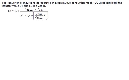
    We ran some numbers and it appears that, in order to maintain a ripple current above 0.5A, both the 15W and 2W designs would run in DCM, according to the following equation from SLVA442 document:

    How do the various equations change for DCM since most of them seem to be based off of assuming CCM?

    Doesn’t operating in DCM result in higher noise due to ringing on the switch node as the inductor current decays to zero?

    How does one go about compensating for a design that sits in DCM?

  • Hi Paul,

    I don't have a rule of thumb but it requires a very low power application for this to be a concern. If it is an issue a gate drive resistor can be used to reduce the current for turning on the FET in most applications.

    What are the input and output voltage/current requirements for each design? Depending on these I expect it will make the most sense to do a CCM design for the 15W.

    You are right DCM does have the additional ringing. This could add some more noise to the system. But I say DCM can have better efficiency for the lower power design because it will allow you to use a lower inductance which is typically is lower DCR.

    Compensating for a SEPIC topology is not the simplest to design for with calculations because it is challenging to model and simulate. Typically calculating the values using the equations for a Boost design will give something which works and with testing a real circuit you might find it needs to be improved or works as needed. As for compensating in DCM, with current mode control a design which is stable in CCM should be stable in DCM.

    Best Regards,
    Anthony

  • Thanks again Anthony!

    Can you please take a look at the attached spreadsheet?

    I am not sure that we can do what you are saying.  We're looking for recommendations if possible.

    Paul

    5417.Design Calcs.xlsx

  • Hi Paul,

    Hope you are enjoying the holidays!

    Do you plan to use a coupled inductor in your application or two seperate inductors?

    If you plan to use a coupled inductor, taking a look through you're spreadsheet I found there is an error using Equation 7. It is missing a factor of 2 in the denominator to account for the decreased ripple when using a coupled inductor. This cuts the minimum inductance for CCM operation and the minimum ccm current in half.

    Looking through some previous designs, the lower power SEPICs with the TPS40211 (or TPS40210) have been designed for CCM with an inductor value in the hundreds of µH. Too little ripple should not end up being a concern. For examples please take a look at PMP2778 or PMP5908. These designs use a 10 and 20 ohm gate drive resistor reducing the current when turning on the FET.

    It appears you are using the TPS40211 to drive some LEDs. Do you plan to regulate the current similar to Figure 29 in the datasheet?

    Best Regards,
    Anthony 

  • Thanks so much Anthony!

    Especially for all your diligence and feedback so far!

    For reference, we will be using a coupled inductor, so we will update the equations.

    So, how does the gate drive current and minimum ripple go from being a problem in our previous dialogue to no longer being a problem?  I just want to understand what the constraints are for proper operation.  I understand how some series resistance can be added; however, there is a limit to how much on the high end to allow the transistor to turn on / off and how little on the low end so as not to disrupt the feedback.  Does the filtering on the sense line take care of the gate drive current pulse? 

    Thanks again!

    Paul

  • Hi Paul,

    I'm glad to help.

    I originally overlooked that the gate drive resistor helps to reduce the peak current during turn on of the low-side FET. The filtering does also help to reduce the spike in voltage at the ISNS pin. The other application had an issue with this because the higher voltage FET would turn on too slowly if a gate drive resistor is used. The larger FET also required more current to turn it on. The size of the gate drive resistance can be selected by testing to see what works. The issue is only seen if the sensed voltage from the peak current from turning on the low-side FET is the same as or higher than the peak current in the inductor. This would case the PWM comparator to inadvertently trigger due to the current at turn on of the low-side FET.

    This current can also be seen in transient TINA simulations. Please see below for an example of this of this. The screenshot is taken with the original boost design and a 100mA load. Notice the current spike is also filtered before it becomes a voltage at the ISNS pin. With 0 ohms the current spike is 250mA and with 10 ohms is 200mA.

    Best Regards,
    Anthony

  • Hi Anthony:

    Is there a TINA schematic available for a SEPIC design using the TPS40211?

    If so, then I could just plug in my component values and go from there?

    Thanks again!

    Paul

  • Hi Paul,

    There isn't a reference TINA schematic available but it may be possible. I tried some but I think the challenge is to have a good model for the coupled inductor to get this to work properly. An ideal coupled inductor causes ringing on the input however the output does regulate. I couldn't find an existing PSPICE model to use as a good starting point.

    Best Regards,
    Anthony

  • Thanks Anthony.  Customer is wondering if you can send us what you have now?  The know its not complete or perfect but would give them a good starting point.

    Thanks,

    Rustin

  • Hi Rustin,

    Attached is the design I left off with. I based it off PMP5910. My goal was to model the coupled inductor as a flyback transformer.

    5367.TPS40210_SEPIC_attempt.TSC

    You will see there is a lot of ringing initially but it settles out. But the inductor current doesn't have the shape I expect when it settles out.

    Best Regards,
    Anthony