This thread has been locked.

If you have a related question, please click the "Ask a related question" button in the top right corner. The newly created question will be automatically linked to this question.

LM2588 Workbench-Design doesn't meet specs

Other Parts Discussed in Thread: OPA454, LM2588, LM5000

Hi,

I used Workbench to design a +-30V out, 9-36V in supply using flyback topology, delivering about +-10mA. I need low ripple, because I use this supply for OPs (OPA454).

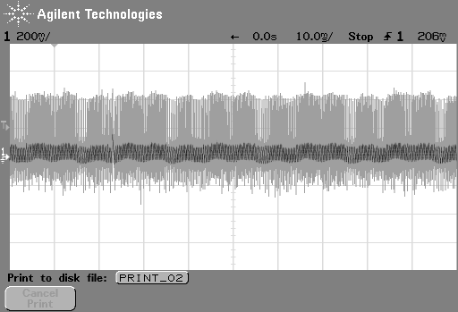
Basically the circuit is working, giving +-30V, enough current, no heating, but, also a lot of ripple.

The ripple voltage is depending of the input voltage, 9-21V, its about 100mV, and low frequency, 21V-24V ripply amplitude jumps up to some hundrets of millivolts, at 24V amplitude drops and frequency rauses, at 28V its quite nice.

Any idea? I add a big capacitor to the output, but no change.

I have some files, showing the workbench output, the realization, and shots of the scope, but no chance to include this files here.


Thanks for helping.


With best regards


Gerhard

  • Hi Gerhard,


    Can you post the schematic you received from Webench?


    With a flyback layout is very important to noise reduction.  Can you also post your layout?


    Regards,

    Marc


  • Yes, of course, but how?

    Lets try. Ah, 'Insert file'. Ok.

    As far as I can see, this noise is caused by oszillations of the control loop.

    1440.DCDC 9 - 36V in +-30V 100mA out dual self made.pdf

    0474.Dual HV Supply.pdf

    Shots:


    9V in, 30 V out at 10mA

    28V in, 30V out at 10mA.

    I used as electronic ballast, but I also tried it on a pure resistor. The scope is AC coupled and no BW limit.

    Thanks for helping.

    With best regards

    Gerhard

  • Hello Gerhard,


    Marc and I just discussed a few aspects of your design. First a cautionary note. If you are using a 1:1 turns ratio from primary to secondary the the peak swithc voltage will 30V + 36V = 66V which is right at the rated switch voltage limit for the device. But I haven't seen your schematic yet to see if this is the case. The second thought is that the rated switch current of hte LM2588 is 5A which os much larger than you actually need. My initial thoiught is to recommend the LM5000 product, which would be a better match to the application, but it is in a very different package if that matters.


    I think the output ripple you are experiencing is due to that fact that the application is very lightly loaded compared to what it is capable of producing. As a result, it is skipping cycles. You might try adding a small feedforward  capcitor in parallel with the upper feedback resistor to see if that helps. (100pf to 1000pF as a starting point.) 


    Marc and I look forward to helping resolve your application issue.


    Alan Martin

  • Hi Alan,

    here is the potential at SW:

    Here the voltage at SW pin. Doesnt exeed 30V, hope that is within the margins.

    The transformer is a universal inductor having 6 equal coils. Two of them in paralell were used for the primary winding and the other four, two in series, were used for the two secondary windings. Hope this gives the planned ratio of 1:2.

    I never designed a flyback regulator before, so I am a newbee.

    I will try the little capacitor tomorrow (it   is 23:30 local time here).

    I also deteted very high current peaks at the input, disturbing my lab supply, and lots of HF, I will try to trace that tomorrow. I also will measure the current needed by the rest of the design, maybe I have to fine tune the design.

    Fortunately the rest of the design is fully differential, so the (differential) signals looking pretty well, but there is lot of potential to make it better.


    With best regards


    Gerhard


  • Hi,


    oh, just forget. The input capacitor C2 is missing on the layout accedently and is put on later. So electrically, the capacitor is there and it is at the free place behind the input connector, were it was planned to be.


    Sorry for that.


    With best regards


    Gerhard

  • Hi Alan,

    I tried out 470p amd 1n. With 1n paralell to R3 (upper feedback resistor) the output is quiet, 20mV ripple at 0mA load. As I add the load, the ripply is quite high, some hundrets of millivolts?? Using 470pF only solves the problem for higher input voltages. Inputvoltages smaller than 14.5V giving the same ripple with or without capacitor.

    I decide to add 1n2, which I have as 0805 SMD and can easily piggy packed upon R3.

    After some investigations I found:

    Between 9 and 13.1V input and my load the total output is 59.998V and ripple ~50mV, but high frequency, so DMM integrates it out.

    Between 13.2 and 14.9V input the ripple is some hundred millivolts, which gives uncertain readings of the voltage, but it must be something around 60.2V

    Between 15.0V and 28V input the output is 59.998V again and ~50mV ripple.

    The ripple is mostly like a square,  frequency is 250kHz.

    I guess, that after adding the 1n2 capacitor, the compensation network has to be fine tuned. Or am I totaly wrong?

    But how and in which direction?

    With best regards

    Gerhard

  • Hi Alan,

    ok, after playing around, I end up with 200nF paralell to R3 (upper feedback resistor) and now the supply is quired without load over the full 9V to 28V input range and also with my load. The output of my amplifier (fully differential) is also quiered and I just start analysis of noise and everything else.

    Hope this will not bring some instabillity into the design, because the feedback network is now capacitive ....

    The rest of the noise seems to be only of high frequencies, so I have to enhance the output filter, but I think, this isn't a problem.

    Do you think, its working now, or have you some other idea to make it stable and reliable.

    With best regards

    Gerhard

  • Hi,

    The "OPA454" Op amp is used as a comparator in  my design. The inverting terminal is connected with 0.7 volt and non-inverting terminal is connected with 0.4 volt with open loop configuration.The V+(POWER SUPPLY) pin is connected with +28 volt and v- pin is connected with ground. The E/D pin is connected with 5V supply through the 4.7K pull up resistor and SF pin connected with V+ through the 3M pull up resistor.


    Now the output of the op-amp is +26 volt. If inverting terminal connected with 0V and Non-inverting terminal connected with +0.4 volt the output goes to zero.Let me know,is there any issue in the op-amp act as a comparator.


    Regards,
    Rajkumar.M
    DATAPATTERNS PVT LTD
    CHENNAI

  • Hi Rajkumar,

    This is a power supply forum.  Please repost your opamp question in the amplifier forum.

    Regards,

    Marc