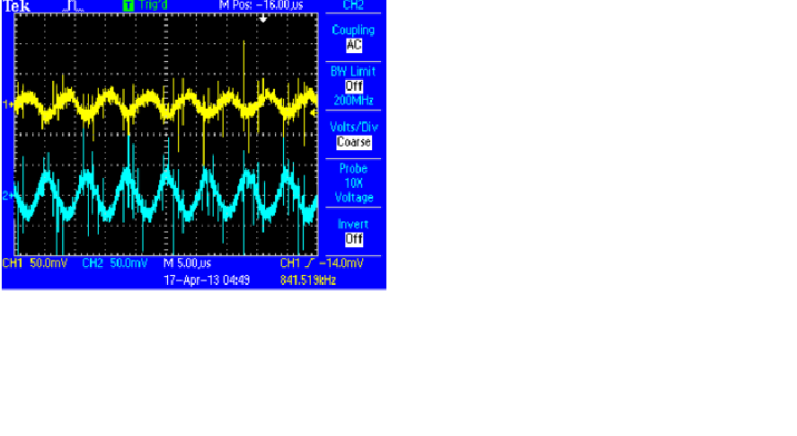
I have started testing the TPS61071 evaluation board which is set up for an output voltage of 5.05V as the default. Everything seems to work fine except when I increase the input voltage to a value >4.7V, the input/output voltage ripple increases to 50mV p-p for the output voltage and 100mV p-p on the input voltage rail. I have included images for the Vin of 4.7V that has minimal ripple and 4.8V which has the increased ripple. The scope CH1 is TPS61071 Vout and the CH2 is TPS61071 VIn, using short scope probe leads. The Vin to the evaluation board is being supplied from a E3631A Agilent linear power supply. There is no load applied to the TPS61071 output.
Vin=4.7V
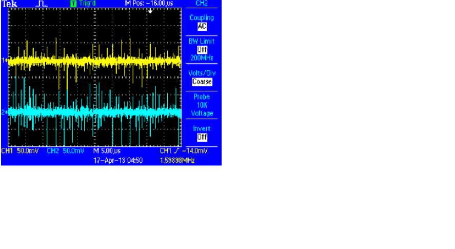
Vin=4.8V