This thread has been locked.

If you have a related question, please click the "Ask a related question" button in the top right corner. The newly created question will be automatically linked to this question.

LMR14203 doesn't work when Vin above 6.6V

Other Parts Discussed in Thread: LMR14203

I have a design using the LMR14203 but I only get the desired voltage across the very low end of the Vin range and in that range the diode gets hot.

I am at a loss to explain why the circuit doesn’t work so I am hoping someone can figure it out. This is a very simple circuit but perhaps there is something simple I am missing???

Inputs to WeBench: Vin7-32V, Vout=5.0V, Iout=0.1A, Ta=30C.

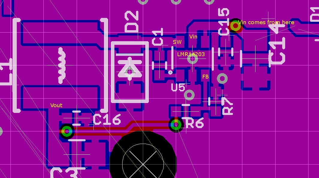
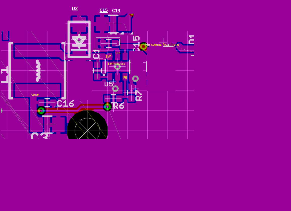
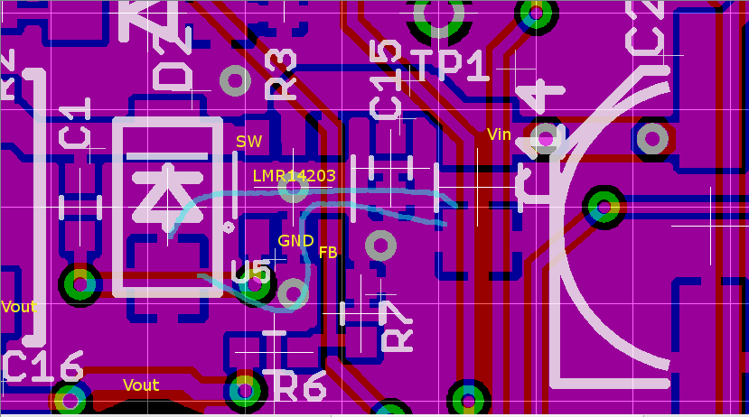
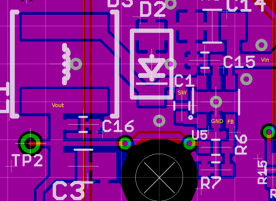
5282.LMR14203.docx has details, schematics, layout and scope shots.

The problem is:  When Vin is between 5.3V and 6.6V, Vout is 4.6V (but not 5.3V) and the incoming power is drawing 250mA so somewhere the power conversion circuitry is wasting 150mA. When Vin is above 6.6V I only get 0.4V out and the circuit doesn’t work at all. The current from Vin drops to 40mA in this range.


  • Hi Eric,

    Here's some preliminary feedback reviewing your post and PCB layout.  For a switching regulator you always want to minimize the input and output current loops and provide proper decoupling at the input pin.

    1) LMR14203 datasheet recommends a low ESR, ceramic capacitor to be placed close to VIN

    2) I only see a 100uF tantalum connected with a "thin" trace to VIN - thin trace will add parasitic inductance creating very poor decoupling

    3) It's not clear to me where your Cout (C3) is being placed, so I can't tell how you grounded this cap

    4) I see FB resistors R5 and R6 and a testpoint TP2, is this where you're tapping the output voltage from? The FB line needs to be kept away from noisy SW trace signals.

    Things you might try to get to root cause:

    1) Solder a ceramic 1uF - 2.2uF/60V from VIN pin to GND plane

    2) Also try to reduce the CB capacitor from 1uF down to 0.15 uF, since you're operating at high duty cycles

    3) Stick with the 15uF or 22uF inductors, don't go higher or lower than these values

    Best Regards,

    -JP

  • Hi JP,

    Thanks for the feedback. I tried hand-soldering a 1uF cap between Vin and GND but there isn't much space available in my current layout. It didn't solve the problem but I can still see 1V 5ns glitches right on the Vin pin. The short lead to the cap has a much smaller glitch but I can't get it any closer.

    Sounds like the LMR14203 is sensitive to glitches on Vin so I have redesigned my circuit with 2 additional ceramic caps on the input and an additional HF one for the output. I've also rearrange the layout to really optimize the paths and keep SW well away from FB.

    Please comment on this layout and suggest any improvements. I'm expecting C14&C3 to be 22uF and C15&C16 to be 1uF. I'll go back to the 22uH for L1.

    Thanks for your input.

    Eric

  • Can someone comment on this layout before I send it out?

    Thanks

  • Hi Eric,

    Sorry for the delay. Your post slipped through, thank you for your patience.

    Your layout looks great! I don't see any cause for concern. I would increase the trace widths for all the caps to as much as allowable. Especially C1 (between Cboot and SW) and FB resistors traces and connections between the resistors.

    That said, I don't see any other cause for concern. I would use .1uF instead of 1uF for the C15 and C16, but this varies by layout compensation needs and it is only a suggestion. Please ensure all the caps especially C1 is rated for double the required voltage (Cboot cap needs to be at least 50V rated).

    Thanks,
    Anston

  • I would look at rotating D2, C14 and C15 by 180 so that all of there grounds connect with copper on the top layer.  This should help with noise by decreasing the input current loop.

    Regards,

    Marc

  • Hi Marc,

    How important is it for the GND pin of the LMR14203 to be close to the diode?

    See the revised layout. I swapped D2 and C1 (Cboot) to make the GND pin of D2 to have a clear path on top copper to the GND pin of the LMR and the input caps.

    If the GND pin of the LMR doesn't matter, then I'll use your layout ideas instead. Your design has the GND pin of D2 and the input caps to be completely minimized. But the GND pin of the LMR is fairly distant and has to cross to the bottom layer to get there which will of course result in additional resistance/inductance.

    See the attached screenshot where I've highlighted in aqua the GND current paths.

  • I feel that you will get better performance with the layout I suggested.  There are much higher currents in Cin to D2 loop and noise there will be seen in the rest of your circuits.  The ground connection of the part still needs to have a solid connection but it is mostly supplying current for the high side drive and being used as a reference voltage for the FB pin.  This peak current is in the 10s of mA range versus the 300mA range. The vias I see on your layout at the bottom of the feedback resistor divider and at the ground pin should connect to a solid ground plane.  Also this change will allow you to bring the C1 boot cap close to the part again and not need to route on another layer.


    Regards,

    Marc

  • Hi Marc,

    I think this is as clean I can I get with 2 layer PCB and the limited space I have.

    What do you think? I moved most of the wires on the bottom of the board out of the way so there is a solid plane under the LMR.

    Maybe I'll add a few more GND vias.

    Eric

  • Hi Eric,

    The layout looks good! Can you ensure the Via's don't break the path between Vout and R6, please make this trace a  little thicker too. Also adding GND Via's is always a great idea, typically around the feedback node, near GND's of D2, C14 and near or under the GND pad for the LMR. This will ensure a direct path for the return currents.

    Thanks,

    Anston

  • Hi Eric,

    I think it looks clean  Add a Via to the ground right at the bottom of the feedback divider and at the output capacitor.

    Regards,

    Marc