This thread has been locked.

If you have a related question, please click the "Ask a related question" button in the top right corner. The newly created question will be automatically linked to this question.

TPS7A7002 Current at 5.5V

Other Parts Discussed in Thread: TPS7A7002, TPS54122, TPS74401

Hello,

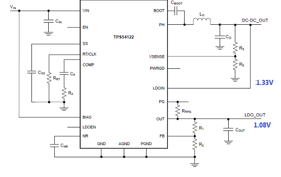
       What could be the max current that could be handled by TPS7A7002 with an input of 5.5V and an output of 1.08V. The datasheet only specifies 3.36A  with VIN = 1.425 V, VOUT = 0.9 × VOUT(NOM).

       I'm looking for a voltage regulator that can handle at least 2A-2.5A with input of 5.5V and output of 1.08V.

Thank You in advanced for any help.


  • Hello,

    The power dissipation is going to be the problem in your case.  At 2.5A and 4.42V of dropout voltage, the LDO would have to dissipate 11W.

    An alternative to the TPS7A7002 that would allow you better efficiency and manageable thermal dissipation is the TPS54122.  The integrated DC-DC converter would allow you to reduce the thermal dissipation to more appropriate levels, while giving you the output of an LDO in one package.

    Best regards,

    Xavier

  • Hi Xavier,

          Thanks for the quick reply. With an input of 5.5V, what would be the maximum current the part can withstand before going to a shutdown mode. How can you decipher this operating range on the datasheet? What parameters should I be looking at.

    Thanks,
    Rodney

  • Hi Rodney,

    As I mentioned previously, it is all thermal.  The thermal protection will kick-in at +160°C junction temperature (p. 7 of the datasheet).  With a 4.42V across the pass element and a theta ja of 46.4°C/W (p. 2 thermal information table) and operating at +25°C, the TPS7A7002 can dissipate 2.9W (equation 3 page 7).  Hence a max current of 0.66A.

    Note that this is not recommended or reliable as the thermal protection temperatrue threshold is not well controlled.  The maximum acceptable junction temperature is +125°C for long term reliability and should be used in calculation.

    With +125°C max junction temp and +25°C ambient, the maximum current the LDO can handle is 0.49A.

    To achieve 2.5A while dissipating 2W, you would need a maximum (Vin - Vout) voltage of 800mV and thus need a intermediate rail at 1.88V.  The TPS54122 will generate the intermediate rail while maintaining a small footprint on the PCB.

    Best regards,

    Xavier

  • Mnay thanks Xavier.

    You mentioned  the TPS7A7002 can dissipate 2.9W (equation 3 page 7). But how did you arrive at 2.9W?

    You mentioned the maximum current the LDO can handle is 0.49A. How did you arrive at 0.49A.

    Best Regards,

    Rodney

  • Hello Rodney,

    To go from the power dissipation to the load current, I used:

    Power_dissipation = (Vin-Vout) * Iload

    To calculate the initial power dissipation knowing only the Theta JA, the ambient temperature and the junction temperature, I used eq.3 on page 7:

    Theta_JA = (Tjunction - Tambient) / Power_dissipation or

    Power_dissipation = (Tjunction - Tambient) / Theta_JA

    With

    Theta_JA = 46.4°C/W,

    Tjunction = +160°C (temperature of the junction at which the thermal shutdown will kick-in)

    T_ambient = +25°C (room temperature)

    you the have:

    Power_dissipation = (160 - 25) / 46.4 = 2.9W.

    Using the first equation above and assigning (Vin - Vout) = 4.42V, the load current then becomes

    Iload = 2.9 / 4.42 = 656mA for the thermal shutdown to start.

    Best regards,

    Xavier

  • Well illustrated. Thanks Xavier. Till next time.

  • Hello again Xavier,

         Referring to TPS54122 Datasheet  

          Theta_JA = 34.9°C/W,  Tjunction = +160°C,  T_ambient = +25°C (room temperature)

                We will have:

           Power_dissipation = (160C – 25C) / 34.9 = 3.87W

           Will my application be only limted to the 1.548V dropout voltage or 875mA load current?

            Pd = (Vin-Vout) x Iout

            3.87W = 1.548V  x 2.5A

            3.87W = 4.42V x 0.875A

            Am I missing something that qualifies TPS54122 for our application of:

                Voltage input = 5.5V, Voltage Output = 1.08V, Load Current = 2.5A

    Thanks,
    Rodney


  • Hi Rodney,

    In the case of the TPS54122, you have an LDO with 200mV max of Dropout voltage for any current below 3A.

    I have reproduced below the spec of interest from the spec table.

    PARAMETER  TEST CONDITIONS MIN TYP MAX UNIT
    VDO(LDOIN)  V(LDOIN) dropout voltage I(OUT) ≤ 3.0 A, V(BIAS) – V(OUT_nom) ≥ 1.62 V 100 200 mV

    Setting the output of the DC-DC converter to a voltage at any voltage greater than 200mV, but less than 1.5V will ensure that you can achieve achieve 2.5A with the device without having any thermal issues.

    For lowest power consumption and good performance (PSRR), I would recommend 400mV to 500mV).  If power dissipation is an issue, but not PSRR then 250mV to 300mV would be sufficient.

    The internal DC-DC converter will convert the 5.5V to 1.3V with high efficiency (say 80%), while the LDO will convert from 1.3V to 1.08V (again at high efficiency since Vin and Vout are close).  Note that the LDO will need a BIAS voltage >= 2.7V (1.08V + 1.62V) to ensure that the dropout stays at less than 200mV.

    Figure 24 in the datasheet shows ~82.5% at 2.5A from 5V to 1.05V.

    So at 80% efficiency and 2.5A, the power dissipation would be 3.37W

    For 2A and 80% efficiency, the power dissipation would be 2.7W.

    With Theta_JA at 34.9C/W, the temperature rise will be ~94.3C for 2A and ~118C for 2.5A.

    You might still need some airflow for cooling the component if the ambient is above 25C.

  • Hi Xavier,

       Thanks for your inputs.

      So I would configure my LDO input to be 2.7V in order to meet 200mV dropout?

    May I know how did you compute 4.22W from an efficiency of 80% at 2.5A?

    If the part will be used at an ambient of 70C (burn-in), with a 118C rise at 2A, will it come to a thermal shutdown?

    At 70C ambient and 1.08V LDO voltage output, up to what current will it be safe to operate?

    Best Regards,

    Rodney


  • Hi Rodney,

    Here is the schematic with approximate voltage you will need to be at.  Note that the BIAS pin is now disconnected from the Vin as your nominal voltage is 5.5V and the Max acceptable voltage at BIAS is 5.5V.

    For the calculation, The output voltage is 1.08V and the current is 2.5A, giving:

    Pload = 1.08V x 2.5A = 2.7W

    Considering the 80% efficiency, this gives a power consumption at the input of:

    2.7W / 0.8 = 3.375W.

    I made a mistake there as the power dissipated in the TPS54122 is:

    3.375W - 2.7W = 0.675W.

    This will give a 34.9C/W x 0.675W = ~24C junction temperature rise over the ambient temperature.

    With+70C ambient, the junction temperature will then be 94C, which is safe under any circumstances for the device.


  • Thanks Xavier. What product can you recommend with a 4A rating for 1.08V desired voltage output?

    Best Regards,

    Rodney

  • Hi Rodney,

    We have two devices with 5A capability.  TPS75501 and UC285-ADJ.  Unfortunately, neither of these is capable of 1.08V output, but are limited to 1.2V.

    Another option is to current share 2x TPS74401 as shown in the attached document for up to 6A.

    8737.TIDU421 - 6A Current sharing Dual LDO.pdf

  • Thanks again Xavier. We are deciding on the value of the components. Do we really need all these components? What would be your recommendation for the rating with our application of 5.0-5.5V input, 1.08V 2.5A output @ 70-85C ambient.

    Thanks,

    Rodney

  • Hello,

         Do you think you can still help me with the requirements. We need to build our boards ASAP.

    Thanks,
    Rodney