This thread has been locked.

If you have a related question, please click the "Ask a related question" button in the top right corner. The newly created question will be automatically linked to this question.

TPS40400 unstable output issue

Other Parts Discussed in Thread: TPS40400

Hi,

I met a TPS40400 issue in customer side.

Input: 12V, Output: 1.0V, f: 600kHz

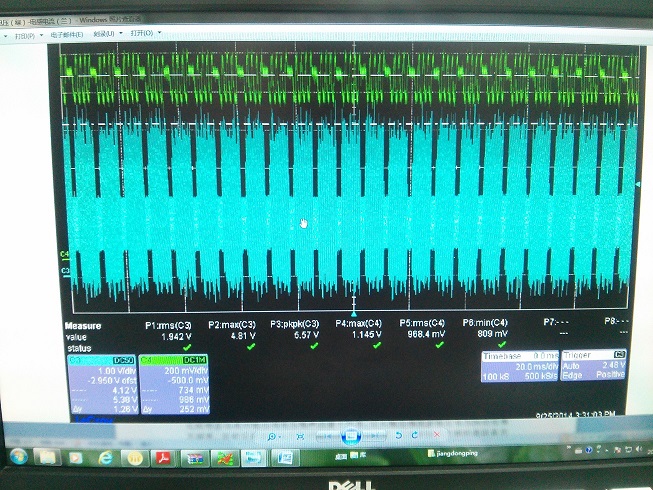
They used TPS40400 solution for DM8167 power. System is okay when powered on. After some time running, TPS40400 1.0V output became unstable as shown below.

The output will ring several cycles and be back to normal. Normal switching frequency is 600kHz. When output is ringing, switching frequency falls to 120kHz and inductor current ripple becomes larger.

I have checked the loop, no obvious issue is found. I suspect that maybe some protection is triggered here.

Please give suggestion here on which protection will lead to below waveform. And other comments is appreciated if you have any idea.

Thanks.

Green: output voltage.  Blue: Inductor current.  All register is in default setting.

  • Can't really tell much from that.  Can you zoom in and also show the SW node?  Also the schematic would be helpful.

  • John,

    Schematic is as below. I can only get this test result now. But we have tried some changes on loop verication, and it comes to the same result. That's why I suspect that some protection is triggered here.

    Thanks.

    Johnny

  • The first thing I would check are the status registers. If a fault protection is being triggered, they will trigger a flag saying what is happening. For starters, just read all the status registers, i.e. STATUS_WORD, STATUS_IOUT, STATUS_VOUT, .... If it's current limit, you'll see the OCF bit set, etc... 

    Are all settings really at the factory defaults?

    • For accurate current sense/protection, you need to program the IOUT_CAL_GAIN register with the DCR of the inductor being used. Also need to make sure the DCR RC time constant in the schematic is properly sized. See the datasheet for equations
    • You may need to also change some settings related to VOUT_SCALE_LOOP. The factory defaults are set up for a 1.2V output. This design is a 1V output.

    One thing I notice about the schematic: There is no VDD-SGND bypass capacitor. 

  • Matt,

    Customer's application does not use PMBUS at all. All the registers are supposed to be at default setting.

    For DCR RC, I have changed RC to much larger value to avoid device from OCP, but the issue is still existing.

    For VDD bypass cap, on customer's board, they place one cap next to VDD-SGND.

    Johnny.

  • Matt,

    For protection, which is latched protection, and which will lead to non latched protection or hiccup mode?

    Thanks.

    Johnny

  • Hi Johnny -

    The point is that the default PMBus register values might not be compatible with their design. For instance, the default value of IOUT_CAL_GAIN is 3mOhms. If the inductor DCR is not 3mOhms, there will be a gain error in the current sensing. Also, the IOUT_OC_FAULT_LIMIT = 10A - i.e. the device will enter current limit at 10A. 

    The TPS40400 has a number of fault protections, most of which have programmable responses. The datasheet specifies default behavior, most of which are set up to "ignore"

    • OC Limit (set by IOUT_OC_FAULT_RESPONSE). 
    • OV Fault (set by VOUT_OV_FAULT_RESPONSE). 
    • UV Fault (set by VOUT_UV_FAULT_RESPONSE). 
    • OT Fault (set by OT_FAULT_RESPONSE). 

    If you can read the STATUS registers by i2c, even if they don't intend to do so in production, the device will actually tell you what protection is triggering, so we don't have to guess