This thread has been locked.

If you have a related question, please click the "Ask a related question" button in the top right corner. The newly created question will be automatically linked to this question.

TPS54225 / Abnormal startup when VIN turn off and on with short interval

Hi,

I found that the abnormal startup when VIN turn off and on with short interval. Please see following background and give your comment for question.
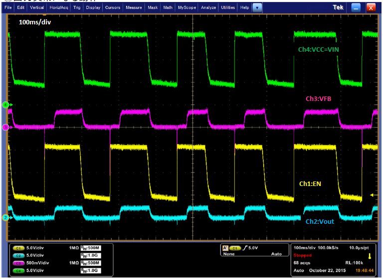
Background

  • The normal startup could be seen when VIN is turned on and off with long interval.
  • But the abnormal startup was happened when VIN is turned on and off with short interval.
  • I guessed this cause is that the converter was restarted before the VREG5 down below UVLO threshold, so I added zener diode between VIN and VCC to keep VCC lower than VIN. See page 2 ow attached.
  • Then I could resolve this abnormal startup issue.

Question

  • Can you please give your comment for the cause of this abnormal startup issue?
  • Can you recommend this workaround that add zener between VIN and VCC? Please let me know if you have better workaround.

TPS54225 abnormal startup.pdf

Your comment will be appreciated.

Best Regards,

Sonoki / Japan Disty

  • Lowering the input voltage partially as shown can cause the UVP function to latch the IC off.  You need to toggle EN or reduce VREG5 below the UVLO threshold.  Placing that zener on VCC will force VREG5 low enough in your case.  It is not a total cure all as there may exist some cases where VIN still drops far enough to force Vout out of regulation but not far enough to trigger UVLO.  I would expect this only to occur at higher output voltages.  Also, now you will require a higher VIN to start up as you have that additional drop and VREG5 is generated from VCC.  So your start input voltage can be as high as 10.75 V.  You will of course also see lower efficiency.  I'll check to see if there are any other drawbacks, but those are two I can think of immediately.

  • Hi John,

    Thank you for your response. As you commented, the waveform of Fig.2 looks like latch off because VFB and VOUT down to 0V. But I do not understand folowing two behavior. Can you see them and give your comment again?

    • Why are VFB and VOUT regulated though regulator is latched off?
    • Why is VFB lower than 765mV that is internal threshold voltage?

    Your comment will be appreciated.

    Best Regards,

    Sonoki / Japan Disty