I am using the LM5113 in a Class S Modulator/Envelope tracker application whereby I am varying the duty cycle/pulse width provided to the 5113 in order to achieve an output from 0V to ~Vdd at the output of the Modulator. This means the duty cycle provided to the Modulator varies from 0 to 95% -- 95% in order to allow recharge time for the top gate driver bootstrap capacitor. The Modulator operates at a 500kHz frequency and the bootstrap capacitance value is 1uF. The 5V power supply is bypassed with 1uF in parallel with 0.1uF. All the capacitors are on the reverse side of the PCB from the 5113 with the shortest connecting traces possible. The circuit works just fine with pulse inputs greater than ~15ns...however, the 5113 output rogue pulses for pulse inputs from approximately 0+ns to 14ns. These rogue pulses are approximately 115-120ns in duration, and they are "statistical" in nature. They are very infrequent coming into and leaving the previously-mentioned band of input pulse widths and occur with the greatest prevalence in the center of that band.
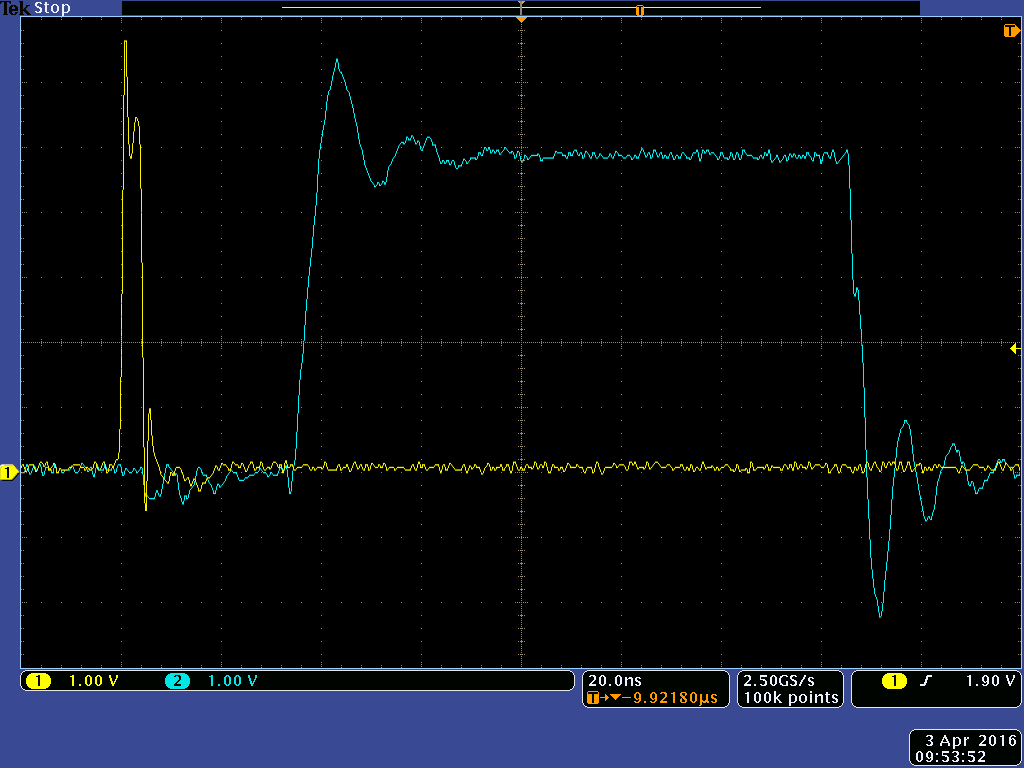
I adjusted the duty cycle to give me the minimum pulse width required by the 5113 to yield an output change. It was approximately 12ns, accounting for noise. It was just before (~4ns) and just after (~14ns) this supposed threshold that the extraordinarily long rogue pulses appear at the top gate drive signal of the LM5113. With some patience, I was able to capture a picture of this rogue pulse as a single shot trace:

The yellow trace is the input to the high side driver on the LM5113 and the blue trace is the output gate drive signal for the top GaN device. Notice that the input pulse is ~4ns wide...and the LM5113 shouldn't even output a signal according to their minimum input pulse width requirement of 10 ns, typical. Yet here we see an output pulse width that is ~115ns long!!! An extraordinary and unexpected value to say the least.
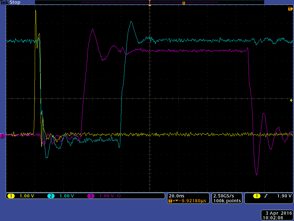
This is better put in perspective by observing the top drive pulse with both the top AND bottom gate drive signals:

In this picture the yellow is the top driver input pulse, the blue is the bottom gate drive signal and the purple is the top gate drive signal. You can see that there is 90ns of solid cross-conduction drive overlap provided in this situation...and this is what is immolating our GaN devices!!! And, according to the operation of the 5113, this shouldn't be happening!
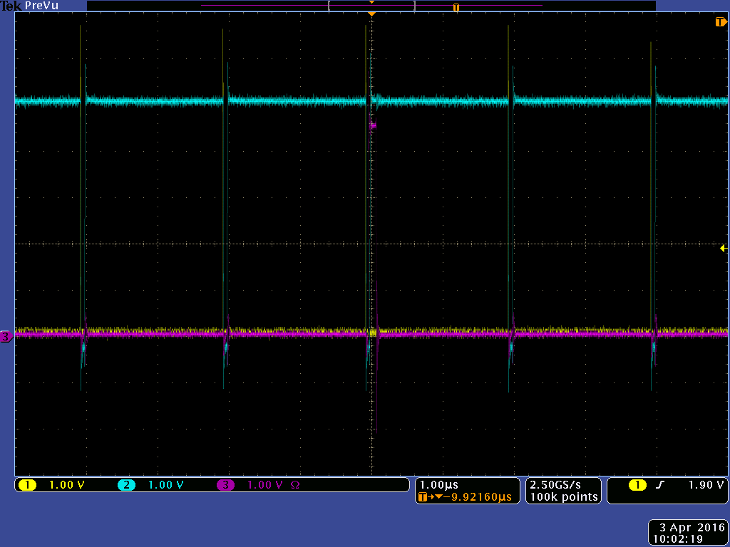
Also, to illustrate the random nature of these rogue pulses, I captured this scope shot of one rogue pulse in a sequence:

In this scope shot you can see the single purple pulse (the top gate drive signal) occurring in the pulse sequence, where none are supposed to occur. This trace represents a 2.6% duty cycle, which again is just below TI's minimum specified pulse width. All it takes is one or two of these long duration pulses to destroy the GaN switches, given the robust cross conduction time provided by the phenomenon.
The funny thing is as soon as the top switch input pulse width exceeds ~12ns, the rogue pulses at the top gate drive signal disappear, and the gate pulse width increases monotonically as they should. There is no obvious or intuitive reason for this VERY elongated pulse to be occurring given the dearth of information about the innards of the LM5113 provided by TI.
These long rogue pulses are destroying the EPC2016 devices being driven in this application by the LM5113. If the input pulse width is kept above the "danger zone" where this rogue pulse phenomenon is observed, the Modulator works reliably, In fact the prototype has been running successfully with a ramping duty cycle of 5 to 95% for more than 100 hours now. I should be able to ramp the duty cycle/pulse width monotonically from 0% or 0ns to the maximum value without destroying the GaN devices being driven. Any insights that you might have into this problem/issue would be GREATLY appreciated. I can brute force implement a means of avoiding this small pulse width band, but the solution is complicated and I think unnecessary, as the LM5113 shouldn't output such long, rogue pulses.

