Because of the holidays, TI E2E™ design support forum responses will be delayed from Dec. 25 through Jan. 2. Thank you for your patience.

This thread has been locked.

If you have a related question, please click the "Ask a related question" button in the top right corner. The newly created question will be automatically linked to this question.

LMZ10505EXT failing at -40C

Other Parts Discussed in Thread: LMZ10505EXT, LMZ10505, TINA-TI

We have had a rash of simple switchers (LMZ10505EXT) failing at cold (-40C). The units work during preliminary test, but fail when the powered on at -40C.  When the regulators are removed, the Vout or Vin will measure shorted to ground.  We have had about 7 failures since 3/21/2016.

Will Cumby

  • Hello Will,

    Please share with us the schematics and conditions for your application.  How are these units failing at -40C?  Is the output voltage not regulated?  Please share any waveforms that you might have captured.  By removing these devices with an uncontrolled hot iron, you're most likely exceeding the recommended max temperature of the package and therefore creating the internal shorts.

    Best Regards,

    -JP

  • I have attached the schematic.  The approximate loads are noted.  I will have to find out if any data was collected before the parts were removed.

    simple_switcher.pptx

  • The techs told me that there was no output voltage on the failed units.
  • It would be good to get some waveforms during a typical test; even on a good unit.

    Also, if you can send us a PCB with a failed unit that has not been de-soldered that would be helpful.  You could send only a partial PCB as well.

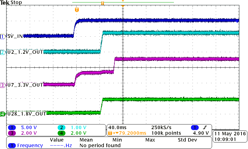
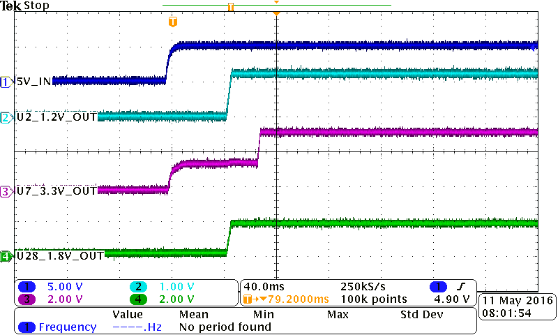
  • I have attached the power up waveforms for cold and room temp boot.  This was measured on a working unit.

    -40 C:

    ROOM TEMP:

  • Will,

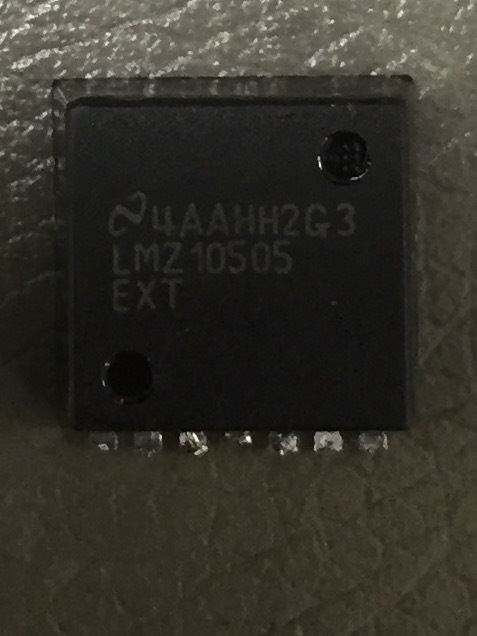
    The waveforms look identical, and normal. What is the top marking on the failed units? Also, please share your reflow profile.

    Thanks,
    Anston
  • I believe all the failed parts have the attached markings.

  • Thanks Will, I'm looking it up now.

    Can you also provide the reflow profile?

    Thanks,
    Anston
  • Your reflow profile is okay and the module passes preliminary power on. This means that the module isn't damaged during placement.

    a) What is the nature of the test?
    b) Are the preliminary tests the same as the -40C tests?
    c) Your schematic looks okay, can you share the layout as well? (I want to rule out parasitics or transients on the input during startup that might cause an overshoot and damage the part.)
    d) Is there any rework or additional process performed to the board after the module has been placed? (Such as a second reflow or hot air soldering etc?)
    e) If the -40C tests are run at room for extended time, will they fail?
    f) Finally, Is power delivery to the board over long cables? How many boards are connected to the same supply? (I'm trying to rule out surges during startup caused due to excessive loading, and inductive parasitics of the long cables.)

    I am exploring every angle, because we haven't seen any failure like this.

    Thanks,
    Anston
  • a) FPGAs on board perform video processing

    b) yes

    c) attached

    f) The box receives 28V and generates 5V to power 3 cards.  The 10505 are on one of the three cards

    If there was a power surge I would expect the 10503 to fail sometimes, but it is always the 10505 that fails. 

  • Will,

    Thank you for the detailed feedback, it helps a lot!

    I've spent quite some time digging and have a hunch its compensation values that aren't quite right.
    Try the following:
    Rfbt = 200k
    Rfbb = 64k
    Rcomp = 1.5k
    Ccomp = 27pF
    Co = 22uF with ESR between 2mOhm and 20mOhm.

    What i think is happening...
    The compensation values you have right now might be conditionally stable @-40C. This might be because the output capacitors change impedance at -40C and throw off the compensation or because the original values aren't sufficient to achieve adequate crossover and phase margin outside 25C.

    I got these values from the datasheet, page 18. Obvious question, why webench has differing comp values?
    I believe, datasheet is more inclusive, catering to tri-temp testing (125C, 25C, -40C) whereas Webench is a corner simulation at 25C only.

    Hope this helps,
    -Anston
  • Would an incorrect compensation network cause damage to the part?  I was under the impression that over current or thermal shutdown would protect the part.

  • Incorrect compensation network could cause oscillation in the system. It could damage the IC when the voltage on a certain pin rings over the rated range.
  • I would think a voltage great enough to damage the part would be measureable.  However, if it is conditionally stable, perhaps only the failed units oscillate.

    The board has a good deal of additional capacitance around the FPGAs, which I think would help with stability.

  • This part is utilizing voltage mode control. It is not necessarily more stable with more Cout. The compensation design should have all the capacitors around FPGA taken into account as part of output capacitors. Please double check the compensation design.

  • Can complex decoupling networks be modeled in Web bench?  If not, is there a spice model for the LMZ10505 that is available for download?

  • Hello Will,
    Thanks for being patient. We are all trying to understand the failure and help solve it.

    The LMZ10505 is a voltage mode device as Yang has mentioned and therefore the internal inductor and all the output capacitors (ones near the load are also output capacitors) will cause a lower frequency double pole and introduce instabilities if not compensated for. Webench usually just suggests the typical output capacitor value and calculates compensation components for that. There are unencrypted Pspice and TINA-TI models available for download from www.ti.com/.../toolssoftware.

    There are a few things I notice on your layout:
    1) You have relief connects to the ground plane on C13 and C45. The C13 is your input capacitor. Having a solid ground plane helps minimize trace inductance which would eliminate potential spikes.
    2) Your power to the IC (5V) is coming through vias. How is it laid out on the board? Do you have an internal plane at that voltage? Or is it a trace coming from a supply?
    3) The upper feedback resistor should be tied to the point of regulation. The way you have it now will result in the point near the VOUT pins of the IC to be regulated. But your load (e.g FPGA) is connected much downstream. Depending on the load, the voltage at the FPGA could be off. Also, how is the output connected to the load? Is it via an entire plane, or a polygon, or a trace? Depending on the connection, there will be additional trace inductance.

    Regards,
    Akshay
  • This thread has been taken offline.