This thread has been locked.

If you have a related question, please click the "Ask a related question" button in the top right corner. The newly created question will be automatically linked to this question.

Hot swap for battery

Other Parts Discussed in Thread: LM5069

Hello all.

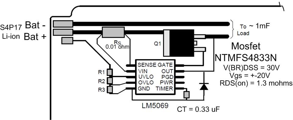
You can see simplified block scheme of my board below.

I want to limit the inrush current which originates from plugging in power supply and battery.

For instance, if I use LM5069 as hot swap controller connected from charger to battery -

it would protect from inrush current coming from battery, but would I be able to charge the battery? It is reverse current according to hot swap controller.

Is there any better solutions?

  • Hi Karlis,

    I was about to recommend a discussion with the battery management team as my (limited) understanding was that battery chargers include input current protection as well as battery-short protection, so both a hot swap on the front end and the back end may not be needed if this is the only component which needs protection.

    Thankfully I checked your recent activity and understand you have already been very engaged with the battery team for your project.

    So is this also for that huge 4s17p battery pack with those nice NCR18650B Panasonic cells? That is one large system and so I can understand if additional levels of protection are desired.

    The LM5069 can allow current in the reverse direction. In fact, the LM5069 typical application uses a single external MOSFET, so the body diode of the MOSFET will always conduct in the reverse direction. Once it begins conducting, the input voltage of the LM5069 would come up and the LM5069 would then turn on the external MOSFET.

    Just keep in mind that the LM5069 does not limit current in the reverse direction.

    Thanks,
    Alex
  • Hi Alex. Thanks for the quick reply.

    Yes you are right,this is for the same projct that I have discussed in battery managent sub-forum.

    Charging current for battery is 10A and discharge is 1A. I wanted to use this chip to protect the board from inrush current when battery gets plugged in. I guess I can use it ,but with good enough mosfet(low rdson)  Do I understand correctly?

  • Hi again. Can you check out my values and approve that this should work?

     Without any inrush current limiter when I plug in the battery the inrush current is:   (dv* Cload)/dt=(15.*0.001)/0.00015= about 100 Amperes

    I intend to limit this to about 5-6A. With schematics like in picture below I get turn-on time about 3,5ms and fault time 15ms. Rsense = 0.01 ohm

  • Hi Karlis,

    It can work but what would be the current going "reverse" from the LM5069's output to input? Note that the LM5069 has an ABS_MAX of +/- 0.3V from the VIN to SENSE pin, so you would have to be careful if current can reach a peak of 30A * 10mohm = 0.3V.

    Other than that, the values you have chosen to start with seem ok.

    I would strongly encourage you to check out our design tools and application notes to help with component selection.

    Here's a short E2E blog to learn how these tools can save you time and avoid problems:
    e2e.ti.com/.../simplify-robust-hot-swap-design-using-design-calculator-tools

    There are useful links to additional resources towards the bottom of that page.

    Thanks!
    Alex
  • The "reverse" current would be battery charging current which is 7,2A in this case.

    Thanks for the link, I will check that out.

  • I did the calculation in LM5069 design calculator excel and watched the videos about this calculator.

    Everything except Derated SOA/PLIM is fine. BTW I wont be using power limiting, only current limiting is used.

    1. Can you please check the added excel file? I can't figure out how to get this parameter above 1.1. 

    2. If I need to use soft-start is it done with the circled components?Also I did not find any information about npn transistor shown in this schematic.

    3. In excel file there are 3 notes. In one of it is is said: "TVS clamp from Vin to GND is mandatory" but in datasheet I don't see this kind of note. SO do I need TVS clamp for voltage overshoot during mosfet turnoff?

    A would really appreciate help because after 15h the schematics and pcb must be done to manufacture it...LM5069_Design_Calculator_REV_B.xlsx

  • Hi Karlis,

    1. Hot swap design is meant to provide protection in case of fault cases. For example, that SOA calculation is used to ensure the MOSFET will not fail if the load draws too much current (such as if if there is a short circuit)

    So indeed this design will be at risk of the MOSFET overheating/failing under a fault condition unless either

    - A stronger SOA MOSFET is used

    or

    - Power Limiting is used.

    Note that power limiting is meant to limit the power dissipation of the MOSFET. It does not limit the power delivered to the load.

    If you set the power limit to 20W for example, then this is what would happen:

    First, let's say the battery is plugged in and is at 16.8V, then if the output capacitors are fully discharged (0V), then the LM5069 will see there is 16.8V initially across the Vds of the external MOSFET. It will start limiting the current to 1.2A. This current will be charging the output capacitors. Once the output capacitors reach 10V for example, then the power limit is still set to 20W, so the current limit charging the output capacitors would be 20W / (16.8V - 10V) = 2.94A

    Eventually it will transition from a "power limit" to the current limit threshold of 5.5A when the output voltage reaches 20W / (16.8V - x) = 5.5A --> x = 13.17V

    So as a result, we would recommend using a Rpwr of ~25kohm resistor to set the Power Limit to 20W. Then use a Ct = 270nF to set a fault time of 12.7ms.

    This would lead to a safer design.

    2. That soft start circuit is used if you wish to have a constant dv/dt slew rate of the output voltage. It does not appear to be needed for this design since it is relatively low current, however if you want to have slew rate control then by all means you can use it. The transistor is a PNP and we recommend a generic MMBT3906 (since it's cheap, but another PNP may work fine).

    3. Regarding the TVS device, this is recommended in order to protect the voltage spike which occurs when the MOSFET shuts off quickly. See this hot swap presentation document (which is geared towards 12V, high current applications, but some material will be relevant). Check out slide 5 in particular.

    6811.2_4_16_Hot Swap Presentation.pdf

    So the input will see a positive voltage spike, the output will see a negative voltage spike. Since the current is very small for this application, the spike may not be enough to damage the LM5069 input. However, since the MOSFET NTMFS4833N has a 30V Vds rating, it would be safer to include a TVS of some sort. Perhaps a "SMA" size device, at least as a placeholder if you have the space.

    Here is an article on TVS selection for hot swap design:

    Thanks,

    Alex

  • Hi again.
    Great answer!I followed your advice and made changes in schematics according to it.
    For TVS I chose this www.elfadistrelec.lv/.../824550181_eng_tds.pdf