This thread has been locked.

If you have a related question, please click the "Ask a related question" button in the top right corner. The newly created question will be automatically linked to this question.

Damaged TPS62160

Other Parts Discussed in Thread: TPS62160

Hello,

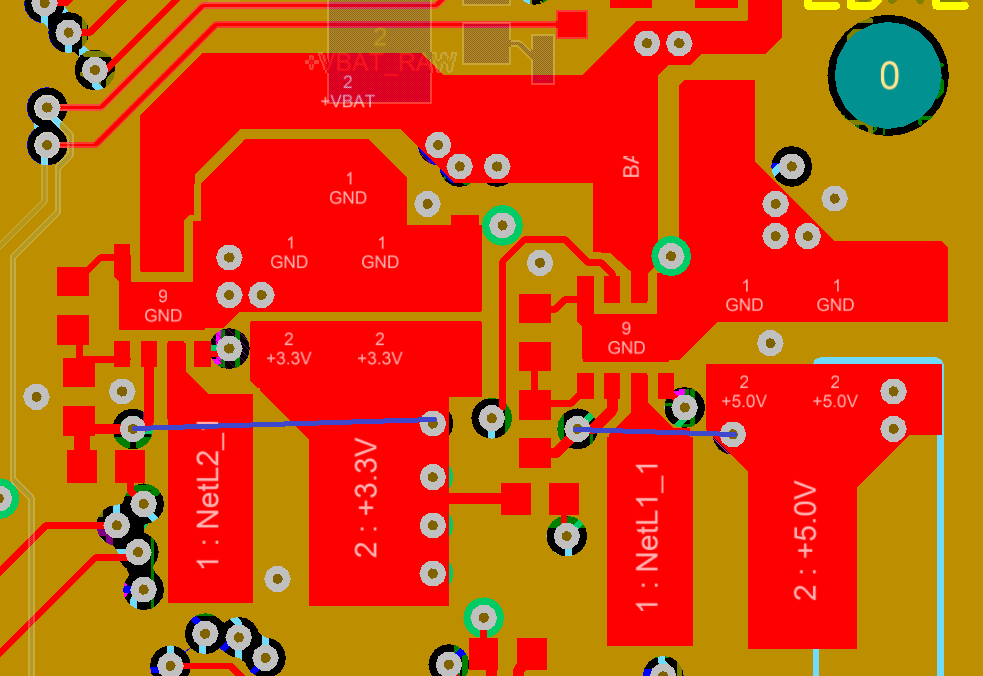
We are currently using the TPS62160 in our designs for both 5V and 3.3V. You can find the schematics and layouts in a previous post here:  

e2e.ti.com/.../481722

We recently ran into an issue where the 3.3V DC/DC seems to be damaged. Our board current consumption is 120mA @ 12V instead of ~30mA @ 12V. The DC/DC gets extremely hot, and after a while the 3.3V will periodically crash/reset (possibly the over temperature protection?)

I measured the switching output (Pin 7 - SW), which is shown below:

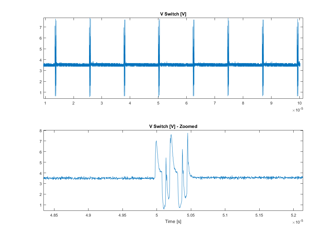
Instead of switching between 0 and 12V, it remains around 3.3V and then does a small burst between ~0 and ~8V. This clearly shows that this chip is malfunctioning. What i'd like to understand is how and why.

We are operating at 12.5V max, and never get anywhere close to the 17V limit. In addition we also have 13V zener diode on the input Vbat in order to protect our electronics against any possible voltage spikes.

Any feedback would be welcome.

  • Quick note. I replaced the chip, and still obtain the same behavior. This makes me ask the question: Is the chip functioning correctly? and if so, what mode is this?
  • There were still some changes required to your design in the other E2E thread. Can you post your final layout and BOM?

    What was your system doing right before you noticed the higher current consumption?

    Is it just 1 PCB showing the issue?
  • This only happened on 1 PCB. Unfortunately, i don't have any information on when this occurred and under what conditions.

    The schematic/BOM was left as is.

    The layout was slightly modified, with the main difference being that the feedback 3.3V is done with a trace, and not directly connected to the 3.3V plane.

  • Thanks for posting. I don't see your BOM in either thread. Can you please list the capacitor part numbers you used?

    How is Vbat applied/connected to the board? Have you looked at this waveform with an oscilloscope? Zeners have a very wide tolerance on their clamping voltage.

    With a new chip, I would expect the current consumption to be lower and the waveform to look better. How does the other rail's waveform look? Do you have other PCBs that you check the waveform and current on?
  • Chris,

    The inductors are SRN4018-6R8M, the capacitors GRM21BR61A106KE19L (psearch.en.murata.com/.../GRM21BR61A106KE19#.html)

    In operation, our Vbat can be very noisy. This PCB serves as an autopilot on a drone with a 12.5V battery. As such, the motor switching causes about 500mVpp of noise, mainly at 32Khz + multiple harmonics. This should still never surpass ~14V.

    However, the tests and measurements that I've shown here are done with a lab power supply. The supply has about 100mVpp of ripple @ ~60Khz.

    The 5V on the defective board seems to work correctly. SW is pulsing between 0-12V with ~55% duty cycle and a load current on the 5V of 100mA @ 12V.

    On another board functioning, the 3.3V SW pulses between 0V and 12V, with a duty cycle of ~28.5%, and has a load current of about 30mA @ 12V (no load on the 5V).
  • Thanks for sharing. Those 10V caps are not sufficient for the Vin caps. They should be ok for the caps on Vout.

    If the failing IC was replaced and the new IC never worked correctly, that points to an assembly issue.
  • The reference i gave were for the Vout caps. the Vin's are GRM219R61E106KA12D (psearch.en.murata.com/.../GRM219R61E106KA12#.html). It's true that they lose a large amount of capacitance due to the DC bias. Could this be an issue?

    Do you have any recommendation on where to look (which components) if it is an assembly issue?

    I'm still not sure how it still manages to properly generate the 3.3V without any pulsing on the SW?
  • Yes, I would say that the amount of effective capacitance at Vin is too low.

    First, I would try re-soldering the IC. As well, take the first IC (which gave the bad waveform) and put it on an EVM or another PCB and see if the waveform is the same.

    It's difficult to read your 'waveforms' as they do not appear to be the output from an oscilloscope. But clearly, it is switching somewhat. I would relook at them with a scope.
  • Chris,

    Thanks for the advice.

    I soldered another chip on the defective board, with get the same defect & observations. Furthermore, I took the DC/Dc from the defective board and placed it on a different functioning board and everything seems to work as it should.

    This clearly shows that i was wrong in assuming that the issue was with the chip itself.

    A visual inspection shows no issues with the soldering of the capacitors / inductor around the DC/DC, and i'm still looking into it.

    I did notice however, that the switching pattern greatly resembles the DC/DC low load mode. I ran a simulation with a load of 10mA which shows the switching pattern:

    webench.ti.com/.../SDP.cgi

    My questions is: How does the chip transition between the different modes (what's the criteria?), and can this give any insight in what might be wrong?

    Alex
  • Final note:

    It was the inductor. Replacing the inductor solved the issue. For some unknown reason, the faulty inductor had value of ~0.2uH as opposed to 6.8uH.

    Thank you chris for your advice and feedback

  • Thanks for posting the solution. Yes, it seems that the inductor was damaged. This sometimes happens to me when I solder them on by hand.