This thread has been locked.

If you have a related question, please click the "Ask a related question" button in the top right corner. The newly created question will be automatically linked to this question.

TPS62171 Power Good Unexpected Behavior

Other Parts Discussed in Thread: TPS62171

Hello,

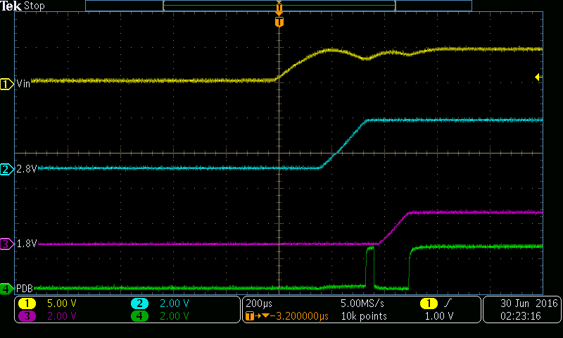
I am seeing an unexpected ramp and drop on the Power Good node of the TPS62171, which controls a RESET pin of a serializer. This PG output must be pulled up to 2.8V for a valid logic HIGH on a serializer, and the output of the '171 is of course 1.8V. I am currently using a 100kOhm pull-up resistor.

I need the 2.8V rail to come on before the 1.8V rail, and the serializer to come out of reset once the 1.8V has stabilized.

What happens is, when the 2.8V rail comes up, this Power Good tracks it, then drops to 0V, then steps up to 2.8V once the 1.8V output has reached its threshold.

However, when I pull the Power Good output up to 1.8V, (not reaching the valid logic HIGH threshold for the serializer RESET), this does not happen, but as I mentioned, the serializer does not come out of reset.

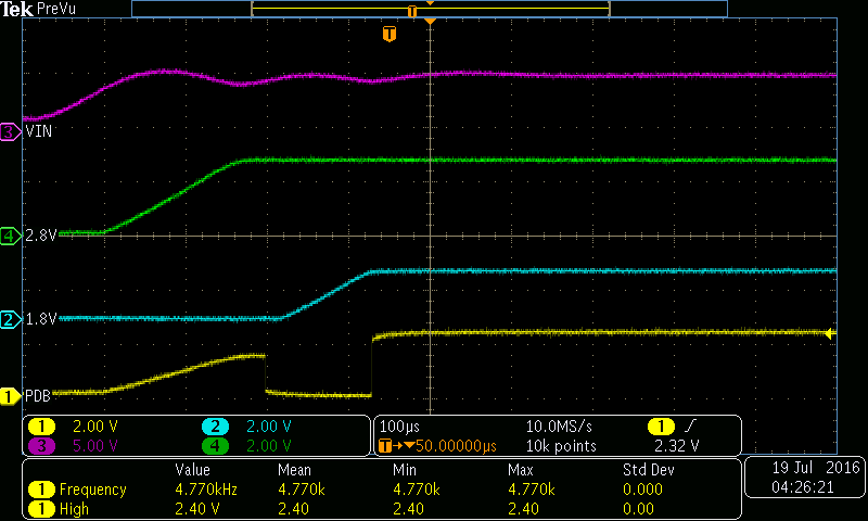
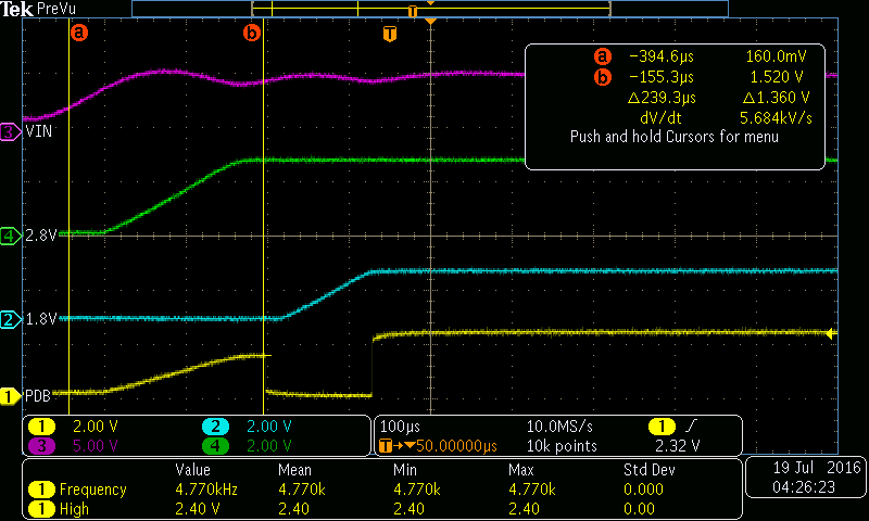
I've attached the schematic which shows the Power Good being pulled up to 1.8V, and the sequencing waveforms.

Please let me know if more information is needed.TIDA-01002 Preliminary Schematic.pdf

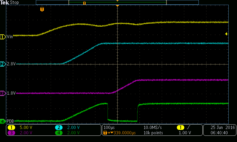
PDB is the same node as PG.

  • Yes, this is expected since PG is high-Z when the device is disabled. You should be able to add a schottky from PG to EN to overcome this.
  • Thanks for pointing out that this would be high impedance until enabled, Chris. That makes sense now.

    If I put the schottky diode 'after' the 2.8V pull-up resistor & PG node, to the PDB (EN) input, would the output ever reach 2.8V, or would the schottky clamp at 0.2V when the PG goes from drain to open? Would this diode go from PG to the 2.8V pull-up & EN node? The input PDB (EN) is pulled-down.

    I can see how the schottky will clamp when the device is hi-Z, but I can't see how the voltage after the diode would be 2.8V, or 2.6V taking the voltage drop into account.

  • Ah, yes. Since you are driving EN with 1.8V, it will try to clamp to this level. But with the 100k pull-up there, it will have a hard time clamping. This is even more true if the pull-up to the 2.8V power good is made lower, say 10k.

    Or, since your logic high is so high (at 2.8V), a regular silicon diode should work fine by keeping PG low enough when EN is low. This should have more drop and be easier to manage.
  • I've provided the updated and correct schematic. It shows the Power Good node pulled-up to 2.8V through the 100k resistor which allows the PDB pin to see the required 1.96V for a valid logic HIGHTIDA-01002 Schematic.pdf.

    You suggest to put a regular diode here:

    Is that correct?

  • No, the diode would connect PG of the 2.8V rail to the EN of the 2.8V rail. This way, when EN is pulled low by the 1.8V PG, the 2.8V PG is held low through the diode.
  • Hi Chris,

    I've updated the schematic and connected a schottky diode from the 1.8V PG/PDB node 2.8V PG/1.8V EN node per your recommendation.

    Thanks so much for your great support here!

  • It looks like the image did not come through. Can you upload your schematic again?
  • 1738.TIDA-01002 Schematic.pdf

    I've attached the updated schematic here. Let me know if it works.

  • Yes, that's what I intended.

    I did recall that you will see a brief high signal on PG once EN is released and goes high. There is some delay from EN -> high to PG being controlled. This is around 50 usec. During this time, PG will be high-Z. Is this too long a high signal for the load?

    If so, we may want to connect the diode to Vout (which should be 0V at startup, if it is discharged. Is it discharged somewhere?) through a resistor.
  • I think that would be too long if the level were high enough.

    Even with the delay, the brief high signal should only be as high as the voltage drop across the diode (0.45V for the diode shown), correct? Then once PG is controlled, it will immediately drop to ground.

    The voltage level which would bring the main device out of reset is around 1.96V

    Am I understanding your concern correctly?

  • The delay would be once the upstream PG releases EN, EN goes up to 2.8V. Now, PG is at 2.8V (its pull-up voltage) for about 50 usec before being pulled low by the second IC.
  • Hi Chris,


    I am seeing some undesirable behavior in the digital blocks of the device which sees the short HIGH from the PG of the 1.8V switcher.

    I have attached an updated schematic which would reflect the change you have described. Please let me know if this is correct.

    If it is, would the resistor in the branch with the diode to Vout (1.8V) have to be lower resistance than the branch with the pull-up to 2.8V?3D_PCB_1to1.pdf

  • That should be keeping any glitch high below your logic high level. Can you post a waveform of Vin, EN, PG, and 1.8V?

    As well, the 10k might be too low and holding the 2.8V high logic level to a lower value. This all depends on the forward voltage drop of the diode you used.
  • Below are some waveforms I took previously when I made added the schottky diode blue-wire into the system. I'm having difficulty including the .jpg/.png of the waveform, so I had to save it into a word docx file. Shown in following order are Vin, 2.8V, 1.8V, and PDB/PG. The PDB/PG waveform shows the delay between EN HIGH and PG control you describe.

    tek0007 - E2E.docx

    Should the resistances be calculated so that the current in both branches are nearly identical? I am having trouble seeing a solution which provides low impedance to 1.8V rail when PG should be low and low enough impedance to 2.8V when PG should be high.

  • The word file was blank.

    The goal is to keep the level low enough when Vout is 0V and high enough when Vout is 1.8V. It won't be 0V and it won't be 2.8V. But it can very likely be kept below your logic high level and above your logic high level based on the Vout level.
  • Did the image above come through?

    The voltage drop of the diode will be ~200mV. As long as the voltage at the PDB pin is above 1.96V, the device will come out of reset.

  • Yep, it came through this time.

    The waveform does not make sense based on your newest schematic. Was this waveform with the new schematic or just with the diode added from PG to EN, as we had discussed earlier?

    Assuming that the 1.8V rail is near 0V when that IC turns on, a 100k/100k divider looks reasonable. The 100k/10k you have in there now is too strong to get to 1.96V I think.
  • Glad it came through.

    Yes, you are correct, this is from the first fix with the diode from PG to EN. I am in the process of setting up the new fix.

    My current reasoning of resistor values is the resistor in the branch of the diode should be small enough to allow enough current to pass to create the voltage drop in the diode. The resistor in the 2.8V pull-up branch should be at least around the same value or less (stronger) to get closer to 2.8V. Is this correct?

    I will update as soon as the fix is implemented.
  • Current should pass as long as the voltage is above the forward voltage of the diode (at a given current, which is quite low). I am considering it as a voltage divider from 2.8V to the 1.8V rail with an additional fixed voltage drop (Vforward).

    Ultimately, you need to get the PG node voltage below 1.96V when the 1.8V net is 0V. And then make sure it is above 1.96V when the 1.8V is around 1.8V.
  • Chris,

    See the waveforms below. Looks like the diode kicked in around 1.3-1.5V, and the voltage at PDB was high enough to turn the device on. After checking with the cursors, it was around 2.3V.


    This looks good, and the ~1.5V is not high enough to bring the device out of reset. I ended up using 10k resistors for both. Thanks for clarifying that the drop occurs long as the voltage is above the forward voltage of the diode.

    It looks as though the 1.8V branch with the diode was a slowed down ramp of the 2.8V, given the additional resistance in that branch. Thank you again for this extremely educational and beneficial discussion here.