This thread has been locked.

If you have a related question, please click the "Ask a related question" button in the top right corner. The newly created question will be automatically linked to this question.

TPS63020 and TPS63051 Schematic Verification

Other Parts Discussed in Thread: TPS63020, TPS63051

Hello all!

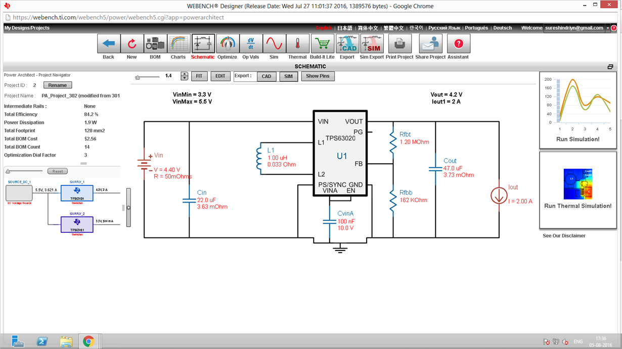
For my first hardware project, I've designed a power supply to power SIM808(4.2V @ 2A Peak) and MSP432(3.3V @ 500mA Peak). Both the regulators are powered by either Li-Po battery or 5V DC supply(selected through P-MOSFET). I simulated the designs from webench and copied the same schematic. It'd be very helpful for me if you can share your comments on the design. This's my first design and I don't have any prior experience in designing hardware. Any feedback you provide will be of great help.432+808_Power.tiff

Thanks

Suresh

  • Hi Suresh,

    I checked the TPS63020 and TPS63051 schematic.

    You connect the TPS63020 enable pin EN to GND. With that the device cannot start. On the first page of the DS you can see a typical application schematic where the EN pin is connected to VINA.

    It looks like you used electrolytic capacitors on the input and output of the devices. If this is the case you have to change them to low ESR ceramic capacitors as recommended in the DS.

    Please provide the updated schematic. I could also review your layout.

    Thanks & Regards,
    Michael
  • Thank you,  Michael for the review. I really appreciate it.

    1. I'll change connect the EN to VINA pin as suggested by Webench.

    2. I'm giving DC input from the AC-DC adaptor directly. I thought of connecting electrolytic caps because, I thought that, they can, to some extent, eliminate the ripple. Correct me if I'm wrong. Can I use ceramic caps, without worrying about ripple?

    As you may've already guessed, I'm very new to hardware designing. I'm reading Analog Engineers Pocket Reference. Can you please suggest me any other resources that complement this great book?

    Layout is not ready yet. Sorry. I'll definitely share it once that's available.

    Thanks again for the help. 

    Suresh

    P.S.: I get it. I'll read the DS completely before starting my design. :P

  • Hi Suresh,

    You need ceramic capacitors very close to device for proper operation but you can add electrolytic caps in addition to to lower the ripple.

    Ok, you can send the layout once it is finished.

    Thanks,
    Michael
  • Michael,

    Extremely sorry for the late reply. Here's the layout. Can you please verify the same?

    Suresh

    2335.layout.pdf

    Power_Schema.pdf

  • Hi Suresh,

    could you please provide a layout plot for each layer? Please include also the silkscreen with the part designator.

    Do you use now ceramic caps in your latest design? In your schematic there are still the symbols for electrolytics.

    Thanks & Regards,
    Michael
  • Michael,

    As per your suggestion, Ceramic caps have been added on input and output sides. But, as you pointed out, they've not been mentioned on the Schematic

    The PCB is only 2 layered. Here's the file you've requested.

    Thanks again for the help. I really appreciate it.

    Suresh

    PCB-LAYOUT.pdf

  • Hi Suresh,

    For buck-boost switching power supply's it is key to place the input and output caps as close as possible to the device pins. The connection/traces on the PCB should be wide and short. Please follow our layout recommendations in the DS for both devices.

    There is only a test point connected to the Power good pin of the TPS63020. If you want to measure the power good signal you need a pull up resistor connected to Vout (or another system rail).

    Thanks & Regards,
    Michael
  • Micheal,

    Thanks for the review. I'll update the same to our Engineer. You've been incredibly helpful throughout. Thanks a ton for all the inputs.

    Suresh