This thread has been locked.

If you have a related question, please click the "Ask a related question" button in the top right corner. The newly created question will be automatically linked to this question.

TPS40304 10-16V to 7V@20A

Other Parts Discussed in Thread: TPS40304

Hello to all,

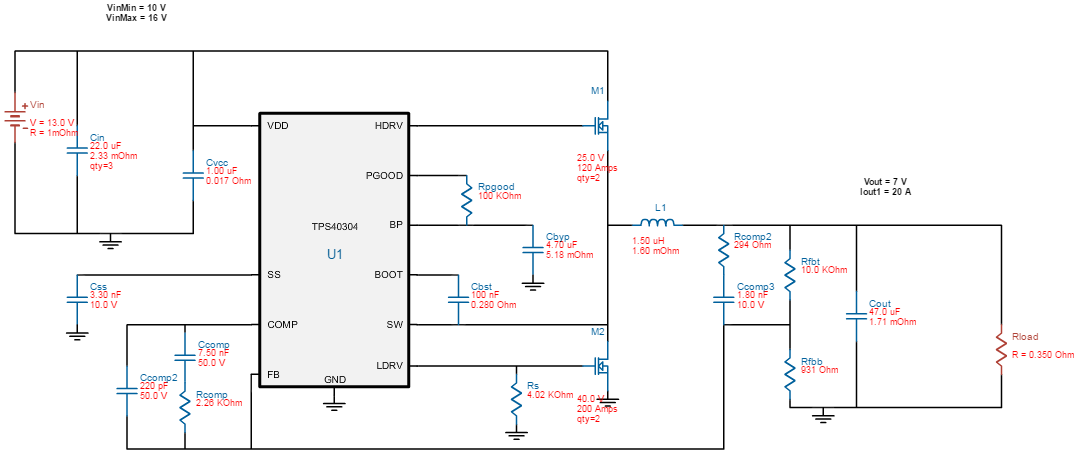
For couple of days I am trying to start that TPS40304, but still no success. I need your ideas and help, so I hope my post wouldnt be ignored :). The initial design is from WEBENCH, but I think it is not correct in some way, as the schematics isn ot working...
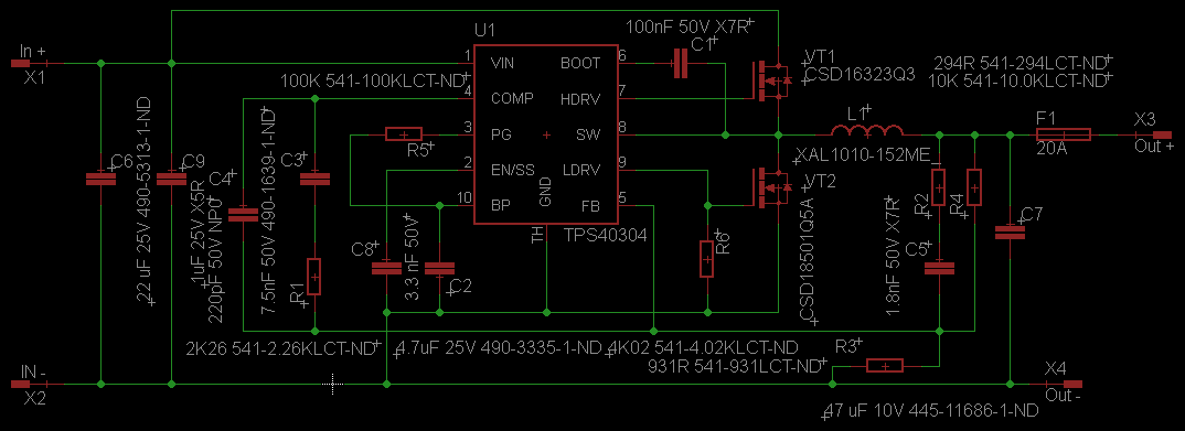
Everything was transfered to Cadsoft Eagle:

Now I have the bunch of PCBs manufactured and parts soldered on. The thing is that it is not working and I would like to get help solving this. On transistor gates there are no control vawe, just a small spike and then nothing. On Css (Webench) or C8 (Eagle) I have steady 5V, so I suppose some part of IC is working. What else should I measure to help determine where is the error ? Can upload the ocsilloscope view if needed.

Best regards

Dainius

  • Hi Dainius,
    Thanks for using WEBENCH. I am looking in this. I noticed that I am unable to create a design for your specs, when was this design created. Can you share your design with me?

    Regards,
    Pavani
  • Dainius,
    WEBENCH has been updated to bring best component selection specifically for Buck Controllers. I have noticed that the design you generated in the past is no longer valid after our enhancements. I will move your question to a different forum so you get support from the experts on this device.

    Can you check if the FETs are conducting and switching?

    Regards,
    Pavani Jella
    WEBENCH Applications.
  • Hi Dainius,
    Did you notice that the WEBENCH recommended design has dual FETs in parallel both on High and Low side, note Qty=2 on the schematic? Your PCB snapshot doesn't show dual FETs. Can you please confirm that your board has dual FETs on high and low sides, both?

    Regards,
    Pavani Jella
    WEBENCH Applications
  • I replied from my email, though I am not sure if that email will reach you, so pasting my letter below:

    Dear Pavani,
     
    Thank you for you prompt reply. The design was created 22 Aug 2016 2:17AM (this date is registered in my projects at myTI). If I understood correctly this should be the link to shared schematics:
     
     
    In case if its not – yesterday I exported PDF file, please find it attached. Strange that Webench generated schematics with impossible specs, but on the other hand I am glad that we helped to find one more thing to correct. Thank you for corrections and moving my question further. I hope to get some comments from there. ,
    About the dual FETs... This was our major head ache here, at our technical dpt. There is a major rule – schematics and BOM in all times must be consistent. Always. As schematics looks quite OK with only with one FET per side, we decided that this is some Webench error in generating BOM (there were some more parts that were only one in schematics and multiple in BOM). But if this is not an error – we think this is not right. All parts from BOM should be present in schematics. Imagine, what would be if I just convert the schematics to Eagle – there will be only one transistor per side. And this instantly gives us faulty board. Exporting (and displaying schematics in Webench) is another issue, that I wanted to report some day. But I’ll try to explain now, hope this is also under your supervision. The displaying of wire junction or intersection is not correct (well, it would be correct like 30 years ago). Maybe noone complained about that, as with some effort this can be ruled out, but that doesn ot make your product better. If you could, take a look at this example:
    We all use the same, “Recommended style” and “CAD symbols”, meaning, that contact of traces is marked with small bubble/dot, and for many years European designers are using this method. In Webench it seems that all traces are not connected, just lying nearby the second trace. But as I said, after some effort this can be corrected. The same issue remains in exported to Cadsof Eagle schematics file. And then Eagle gets confused, so we still have to redraw everything, with standard connections, then it works. From that perspective I say, that export is not working correctly, but this is more linked to initial generation of schematics. And now, knowing that Webench exports schematics with missing parts (as they are seen only in BOM) – this is major fault. If it would be too much trouble – please, enable the dots on connected traces.
     
    As you said – you forwarded my request to somome else, so I think I will wait for some more comments, as even with one transistor per side it should be working. We were testing the boards only with 1-2A load so, its not even near to requested 20A (presuming, that two FETs are only for higher current capabilities).
     
    And once more – BOM and schematics have to be identical.
     
    Thank you for your support and attention, will be looking forward to get your reply.
    ____________________
    With respect
    Dainius
  • Dainius,

    I have moved the post to the Non-Isolated DC/DC forum. They can provide some application specific help/information.

  • Hi Dainius,

    What's the load condition during your test?

    R6 value in your design seems too small for 20A load.

    Can you try a larger value for R6?

    Equation 2 in datasheet can be used to calculate R6 value.

    Thansk

    Qian

  • Hi Qian,

    It was without any big load - only multimeter and a small lamp (5W or 10W, dont remember now), anyway 1-1,5A max.

    R6 is 4K02, but I will only be able to recalculate on Monday (or maybe tomorrow), as now I writing from my smartphone and it is not very convenient to search for all the parameters for equation. I am not even sure I can get all :D. Anyway, this was taken from Webench design, which as I know now was faulty...

    But can it be, the R6 is even too small for TPS to start at 1A load ? Maybe it triggers OCP at once and that is why it is not working ?

    Best regards

    Dainius

  • Hello to all,

    Well, I tried to do some calculation. I attached the Excel sheet  with formula, should be correct. For 20A I should have ~3,4K resistor, with now used resistor (4K02), max current should be about 24,5A. Or am I wrong ? Both ways - I wasnt even near to those currents with my load (roughly 1-1,5A).

    Calculation.xlsx

    Looking forward to get some comments and ideas where to start troubleshooting :).

    Best regards

    Dainius
  • Hi Dainius,

    The datasheet shows a 10uA is flowing through OC resistor (4.02k) during calibration time. Can you check if the voltage on the OC resistor during calibration time is correct?

    Also, can you check LDRV, HDRV and SW sigals during normal operation?

    Please put these three signals in the same waveform.

    Thanks

    Qian

  • Hi Qian,

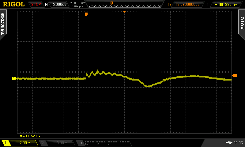
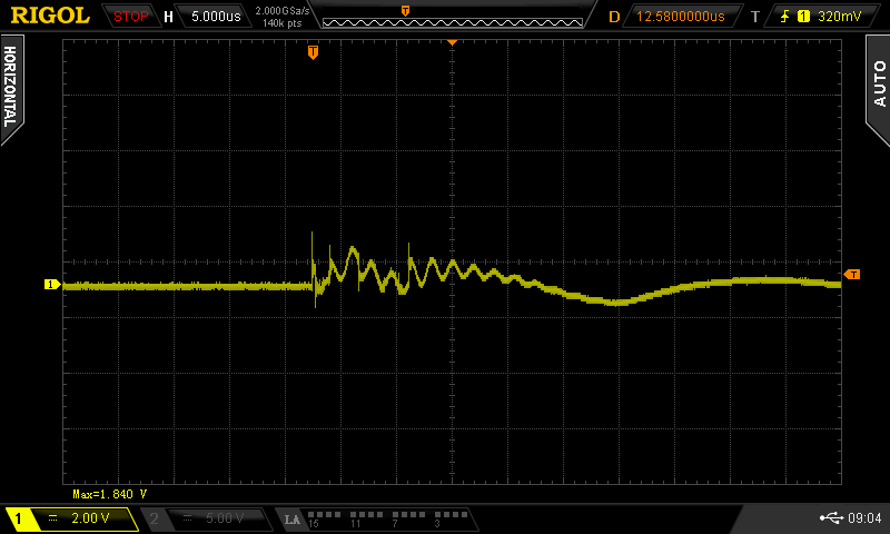
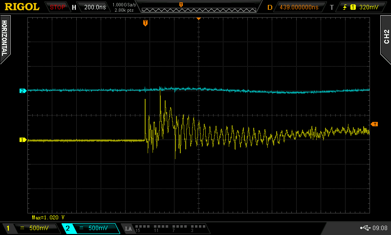
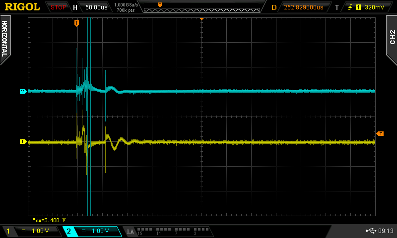
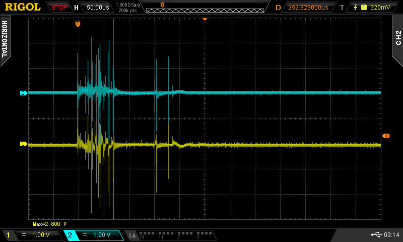
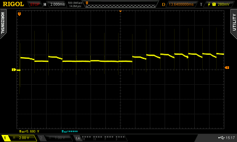
    Heres the voltage on OC resistor, made with single shot trigger, to catch the right moment. This should be the same waveform as LDRV, right ? 

    Though it was quite hard to reach any repeatability, so I made several "shots", some of them are quite similar, so I think those could be correct. Maybe I should use longer period and some more waves would come out ? Anyway, all comments are welcome.

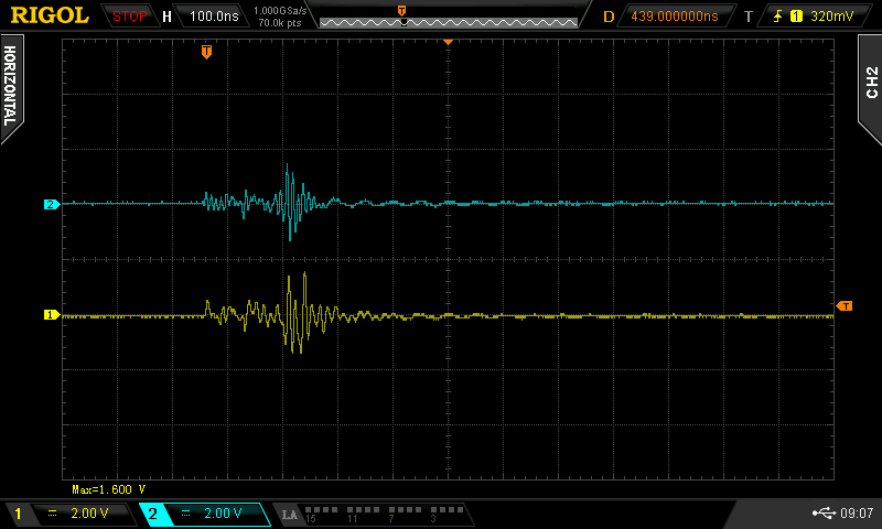
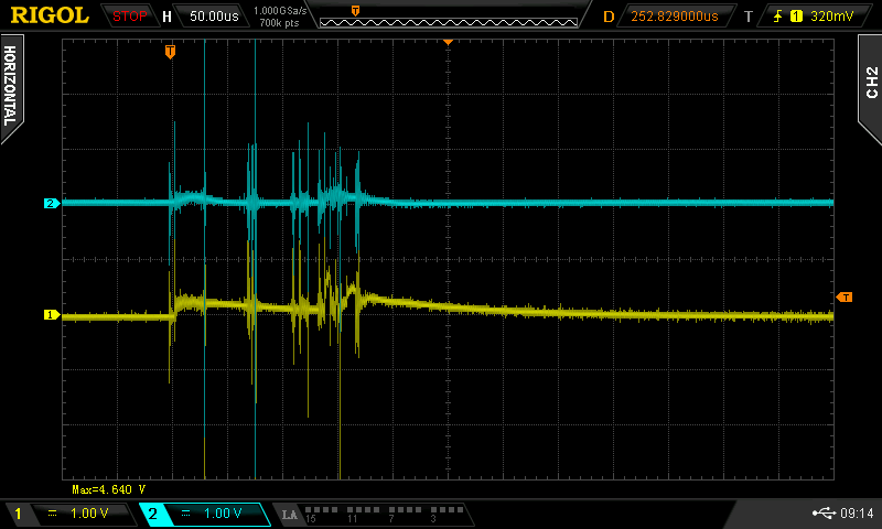
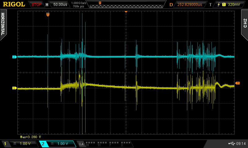
    Ant now some waveforms from LDRV (YELLOW) and HDRV(BLUE). Unfortunately, my scope has only two inputs, so I cant put SW at the same time.

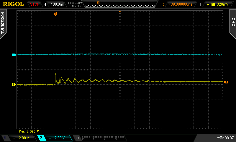
    And here is the SW (BLUE), together with LDRV (YELLOW)

  • I think the TPS chip was faulty. Replaced, after that I had very nice and steady 1,02V on output (instead of 7V!). Measured waveforms:

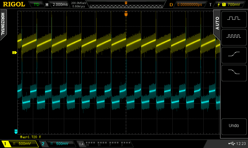
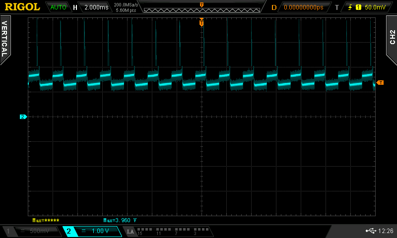
    HDRV - yellow and LDRV - blue. Strange thing, that HDRV would seem normal, ramping up from 0V to 1,7V, but the LDRV acts strange (I think), as it has the sqare wave, but raised for about 1,2V above 0V, I mean its changing from 1,2V to 1,6 (approx.). Closeup:

    While measuring noticed, that TPS chip is getting quite hot, disconnected everything, checked, but everything seems to be OK. Connected, and now there is no nice 1V on the output, on the scope it seems that it just repeats HDRV wave there. Strange things happens...

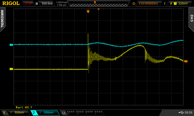
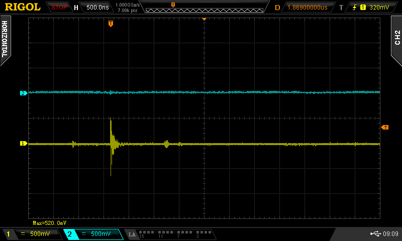
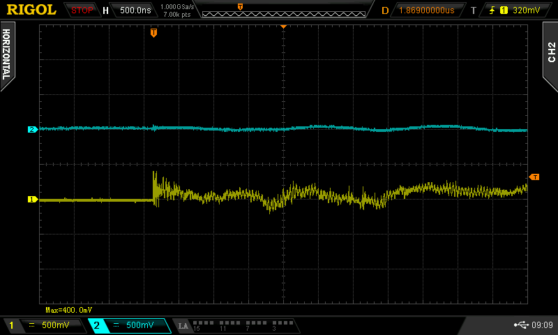
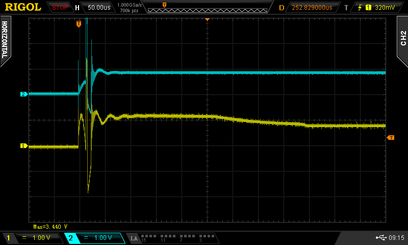
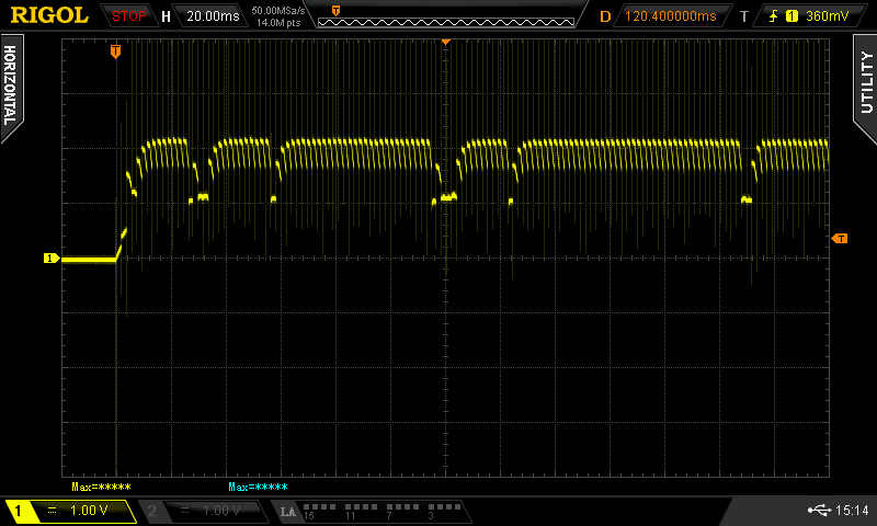
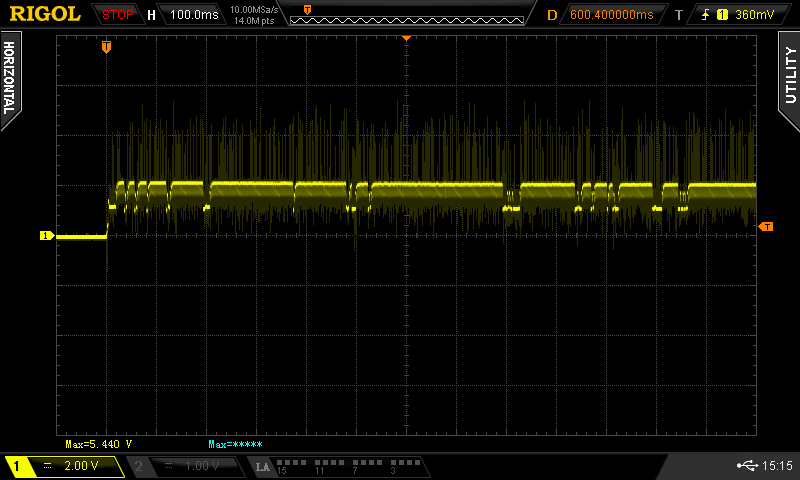
  • It appears, that HDRV, transistor was also taken away by faulty chip, so replaced that also. Now have the following pattern on the output:

    Longer time frame

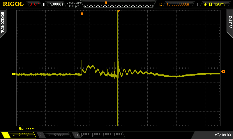
    Bigger voltage scale to see spikes

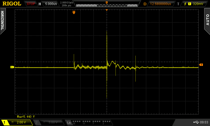
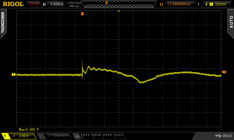
    Zoomin of the output. Device start is at vertical [T] marker (under the RIGOL word)

    Those patterns were measured without any load. Though I can hear the coild "whispering". The sound of heavily overloaded power supply (I hope you know what I mean). The rest of parts are not burned, checked... Chm... Too small output capacitance? Wrong capacitor type ? Output resistance is about 11K. 

  • Hi Daonius,

    The HDRV and LDRV waveforms look not correct.

    Can you double if all components value are correct?

    Also please check if there is any soldering problem.

    Thanks

    Qian

  • Hello to all,

    Well, after few days of testing nothing new. The TPS IC is working, somehow, but basicly the waveform is not correct, though I have the square (or similar to it) wave of both transistors gates. I think the schematics is not working, as the principle is wrong, as Pavani said " I have noticed that the design you generated in the past is no longer valid after our enhancements.". Now when I am generating new schematics with same specs I dont even have TPS40304 in selection list. So I presume, that this IC cannot work correctly in previously generated schematics. I think I give up, dropping the PCBs ant parts that will not be usable in new schematics, and doing the new design in Webench. Pity, lost some money and lots of time :(

    Thank you all for your kind support!

    Regards

    Dainius