This thread has been locked.

If you have a related question, please click the "Ask a related question" button in the top right corner. The newly created question will be automatically linked to this question.

BQ24650: Battery connected to bq24650 in not charging

Part Number: BQ24650
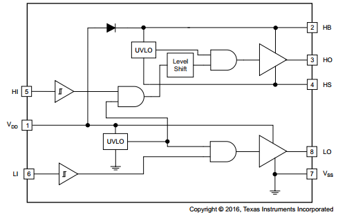
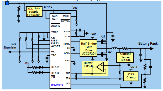
Other Parts Discussed in Thread: CSD18504Q5A, BQ24610, TPS54060, UCC27201

Hello Support team,

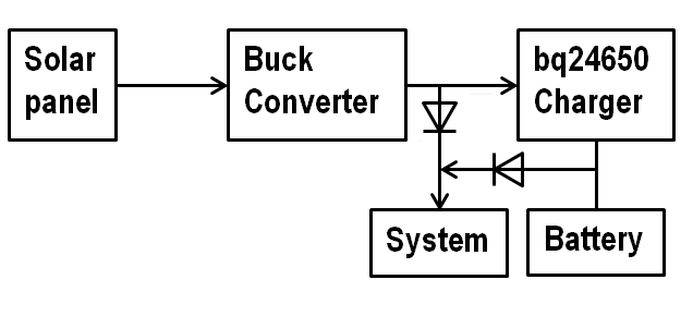
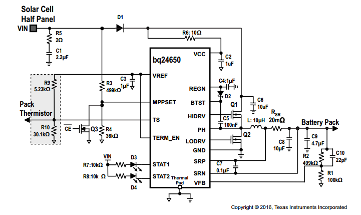
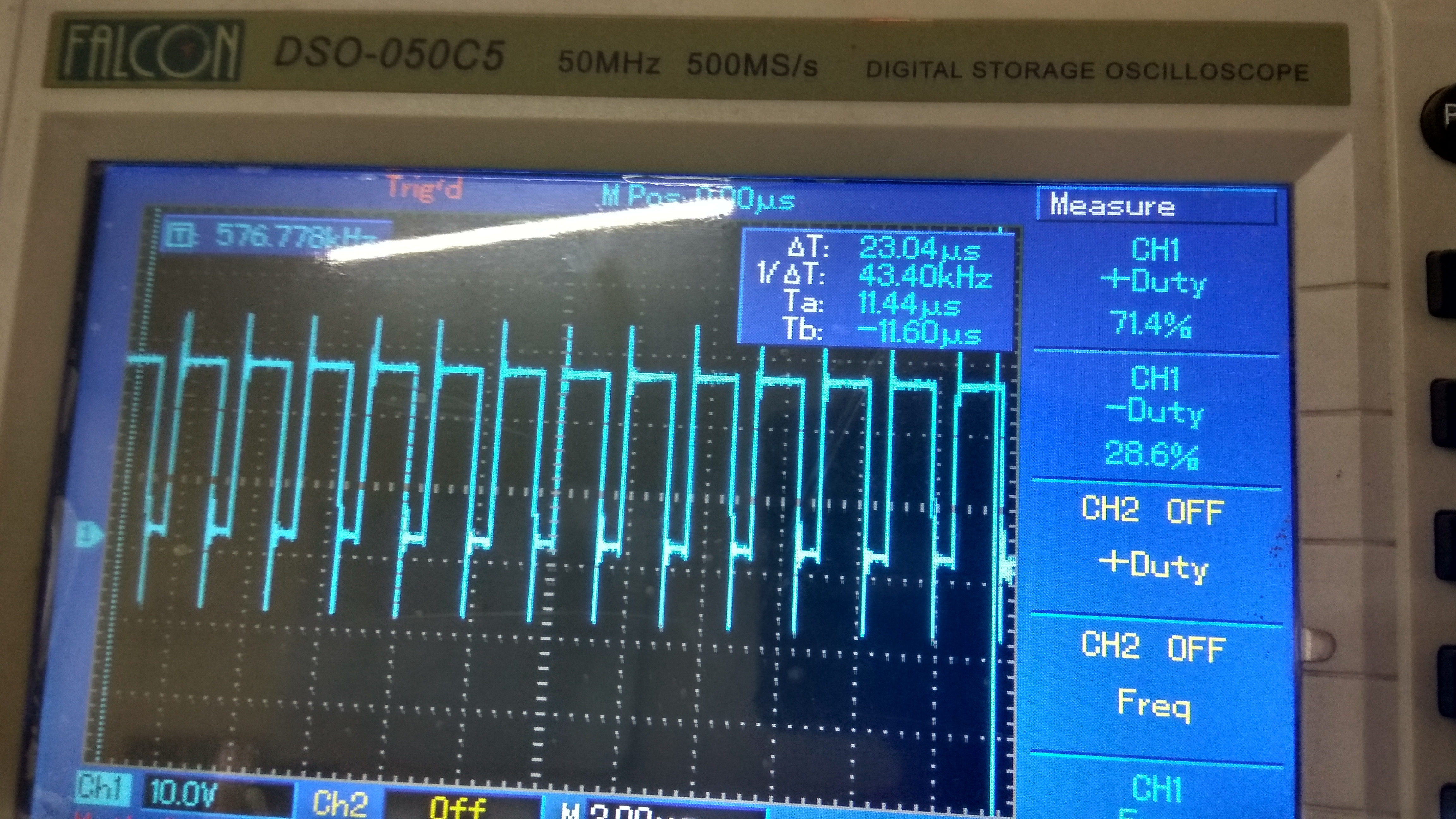
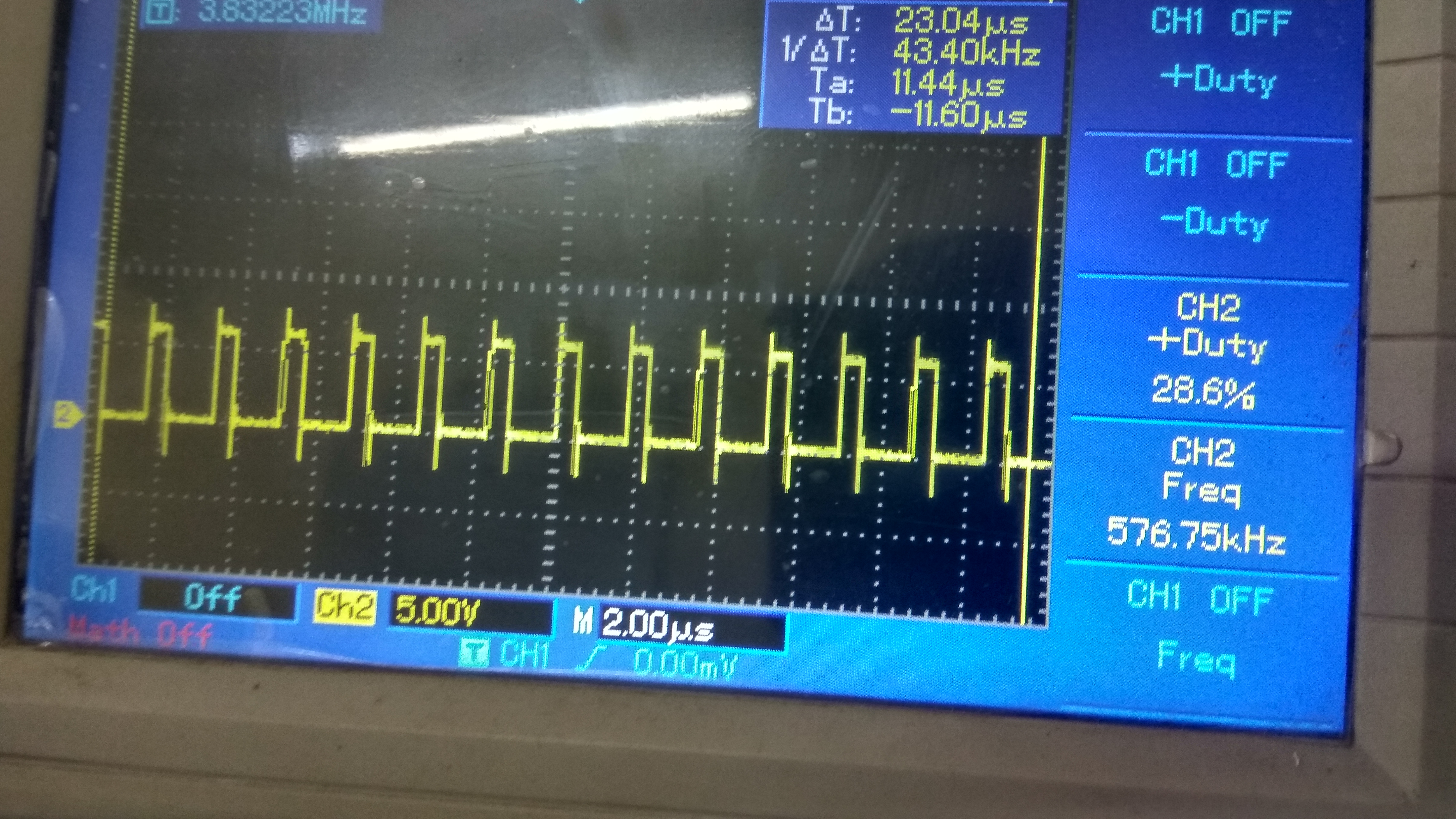
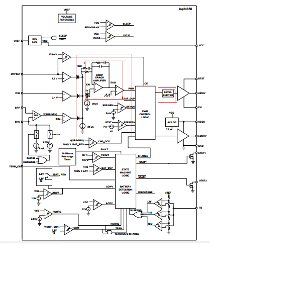
I am using BQ24650 IC for MPPT design,  I have designed for 10A  charging current , rigged up  circuit as shown in datasheet but li-ion  battery connected to output is not charging.

Below are the design details:

1.Vin 12V

2.Vmpp 17V

3.Icharge 10A

I am getting 1.8V on Vfb pin and  2.4V on Vmppset pin.

Please help me out regarding the issue ASAP.

Regards-

Nagaswaroop

  • Hi Nagaswaroop,

    Sorry for the late reply. It's a application note for implementing high input voltage in BQ24610 shown below. It's the same concept to implement on BQ24650. You may add some function block including Vcc bias, half bridge gate drive, current sensing, buffer and voltage clamp. You can follow the concept to add changes on your design.

    /cfs-file/__key/communityserver-discussions-components-files/196/8004.0184.SLVU580_5F00_A-practical-high-voltage-charger-solution-using-bq24610-charger-.doc

    Best regards,

    Ann Lien

  • Dear Ann Lien,

    Circuit configuration you suggest  will it work for charging 24V 15A lifePo4 battery also?.

    Why because the output of TPS54060 is 8 to 14V which is connected to VDD of  UCC27201. In the functional block diagram  of UCC27201, Output of HO and LO are drive with amount of VDD voltage, if we connected 24V battery for charging, gate voltage of high side MOSFET should be more than battery voltage, but on HO pin will get Maximum of 14V only. If  gate to source voltage is not more than 24V how  battery will charge?

    Please do the needful.


    Regards,

    Nagaswaroop.

  • Hi Nagaswaroop,

    High side drive will drive the high side MOSFET by the bootstrap circuit so there is no concern with the Vcc level. Discussed with team, this application would be too complicated to implement on your system. Could you please add one Buck converter at the input to maintain the Vin consistent? It will be easier for your design.

    Best regards,
    Ann Lien
  • Dear Ann Lien,

    Please provide  the reference  schematic for  charging 12V/24V lifePo4 battery and also let us know if you have any simulation tool to simulate the Bq24650 behaviour.   

    Regards,

    Nagaswaroop

  • Hi Swaroop,

    Sorry for the misunderstanding, could you kindly confirm if you have two kinds LiFePO4 battery for 24V and 12V? If yes, the output VFB need to change between different voltage level.

    We have no reference design for your application right now but the function block is like below diagram. You also can refer to BQ24650 typical design schematic in datasheet. On the other hand, you can search the suitable Buck converter for your design spec in ti.com. Do you have bq24650 EVM board? As long as you decide the Buck converter, you can also demonstrate the charger behavior with the Buck converter.

    Best regards,

    Ann Lien

  • Dear Ann Lien,

    Could you kindly confirm if you have two kinds LiFePO4 battery for 24V and 12V?

    We have two 12.8V LIfePo4 battery, while testing 24V battery system we will connect two in series.


    Do you have bq24650 EVM board?

    Yes we have, we currently evaluating function with EVM only.


    And can we connect the LDO having  4V to 60V input voltage,Output voltage is adjusted to 28V and  which can delivers up to 100mA of load current at Buck converter stage?


    Please provide us the simulation tool link for Bq24650.

    Best Regards,

    Swaroop


  • Hi Swaroop,

    Please provide us the simulation tool link for Bq24650.

    We don't have the simulation software for bq24650. But we have the calculation tool on ti.com, hope it could help  you.http://www.ti.com/product/BQ24650/toolssoftware

    And can we connect the LDO having  4V to 60V input voltage,Output voltage is adjusted to 28V and  which can delivers up to 100mA of load current at Buck converter stage?

    Please verify the power consumption of back stage including battery and system. Since the solar panel is the power source of battery and system. Is it enough for 28V/100mA?


    Best regards,

    Ann Lien

  • Ann Lien,

    Please verify the power consumption of back stage including battery and system. Since the solar panel is the power source of battery and system. Is it enough for 28V/100mA?

    I will incorporate only Vcc Bias Supply block(I will use LDO which I previously mentioned) of figure1 in figure 2 to safe guard the VCC and STAT pins, rest of the connections of figure2 remains unchanged i.e I will not use Half bridge gate drive, current sense, Buffer, Clamp.

    Figure 1:Modified bq24610 circuit for high voltage application.

    Figure 2:bq24610 circuit.


    And Let us know how to design EMI filter for Bq24650?


    Regards,

    Swaroop

  • Dear Ann Lien,

    Kindly reply to below mail. Awaiting for your valuable response.

    Regards,

    Swaroop.

  • Hi Swaroop,

    Sorry for the late reply. As we know, the EMI filter is to prevent the switching noise influence AC Bus in typical application. So the charger may not need the EMI filter for the conductive EMI. But the radiation EMI could be decreased by two way, slowing the PH switching slew rate and adding snubber at PH. For your application, you can add snubber at PH node.

    There are also some EMI design guidelines you could refer to:

    To reduce EMI source, please make sure to

    - maximize continuous PGND plan on top layer to decoupling capacitors of key nodes (PH, SRN(VBAT)).

    - Tie PGND pin directly to Power Pad using top layer.

    - Use 2nd layer as PGND with planty of vias to connect top and internal layer.

    - Use array of vias to reduce via inductance (400nH/VIA).

    To eliminate transmitting soruce,

    - avoid long traces close to PH nodes

    - Avoid long traces at the edge of PCB

    To trap radiated EMI,

    - use continuous PGND rings around each layer of PCB to build "faraday cage" to trap EMI leakage

    - Each ring should be tied together using as much vias as possible to reduce PGND impedance

    - No signal should be routed outside of the PGND

    Best regards,
    Ann Lien
  •  Dear Ann Lien,

    1.Is really necessary to incorporate the EMI filter in our design? if so which one we have to incorporate Differential mode or Common mode noise filter ?.

    Please share the design for Differential mode and Common mode noise filter.

    2.For common mode noise filter there are four type of configuration , Which one is  best suites for our application and how ? please find the attachment for different configuration of differential mode or common mode noise filter.

    3.Is Bq24560EVM Incorporated with EMI suppression techniques? if so which are those and can we use the same techniques  for our 12V/24V 15A MPPT design?  

    4.Is Bq24560EVM designed to meet the EMC standards of India? if not what are the changes we need to make to meet EMC standards of India? 

    6.Please explain how to select the right positive temperature coefficient(PTC) for our application.

    7.Please share links on EMI, EMI reduction techniques  and EMC standards related to our application.

    8.Figure 1 and 2 images of HIDRV and LODRV pulses respectively, how to reduce the impulse in HIDRV and LODRV waveforms?

      Figure 1:HIDRV waveform.

    Figure 2:LODRV waveform.

    Please do the needful ASAP.

    Differential and Common Mode Noise.pdf

    Reagrds,

    Swaroop


  • Dear Ann Lien,

    Kindly replay to below mail, awaiting for your valuable response.

    e2e.ti.com/.../2197872

    Please do the needful  ASAP.

    Reagrds,

    Swaroop

  • Hi Swaroop,

    We only add snubber in our design to reduce the radiation EMI problem. For the input filter design, you can refer to this link www.ti.com/.../snva538.pdf

    BQ24650 only has the input filter for RC damping network.

    We use NTC thermistor in temperature sensing, you can refer to datasheet section 8.3.17 and use recommended 103AT NTC thermistor.

    Did you optimize the GND routing for the probe when you captured this waveform? If you did and the result is the same, we could add more Rg to slow down the turn on slew rate to make the impulse small.

    Best regards,
    Ann Lien
  • Dear Ann Lien,

    1.Is Bq24560EVM designed to meet the EMC standards of India? if not what are the changes we need to make to meet EMC standards of India?

    2.Please  explain how to optimize the GND routing for the probe?

    3. what is the amount  of Rg should be added and where we it should be placed?

    Regards,

    Swaroop

  • Dear Ann Lien,

    We are facing delay in your response every time. we request  you to respond ASAP.

    We where getting response less than 12 hours from  previous technical support person which we used to  interact, but its now extended more than 24 hours.

    Regards,

    Swaroop.


  • Hi Swaroop,

    Sorry for the late reply. We were in holiday yesterday.

    For the EMC standard, It is a system level standard. There is not valuable to focus on if bq24650 EVM meet the EMC standard. Even if we pass the EMC standard, it wouldn't meet the EMC standard after you apply the same circuit of our design. It depends on not only charger but also the system. So we didn't let BQ24650 EVM to pass the EMC standard. For reducing EMI, you can refer to the previous post to follow the EMI guideline.

    For the GND routing, did you minimize the GND routing with your probe to decrease the noise? I want to make sure it's not the noise injection caused by test procedure. 

    For the Rg, you can test with 10 ohm first. Please use 0603 size. 

    Best regards,

    Ann Lien

  • Hi Swaroop,

    For the Rg, please also parallel a diode to let turn-on go through the resistor and turn-off go through the diode.

    Best regards,
    Ann Lien
  • Dear Ann Lien,

    1.Where we have to optimize the GND routing, in PCB layout design or in Lab room ground? request you to explain the procedure for both.

    2.Rg should be connected parallel to or series with High side MOSFET gate or Low side MOSFET  gate or to both? request you to mention.

    3.What is the type of diode need to be connected parallel with Rg? please mention.

    Request you to send the example circuit for optimizing GND and for Rg  configuration.

    Regards,

    Swaroop.

  • Hi Swaroop,

    Q1:

    For PCB layout, you can refer to our EVM layout. For test procedure, take our EVM board for example, you can use MOSFET(Q1) pin3 S2 (PGND) as your test GND to minimized the GND routing.

    Did you test with BQ24650 EVM board? Since I tested with our EVM board, there isn't the spike and shown below.

    Or you tested with your design? Could you provide the schematic and layout for us to check if there is anything could cause the spike?

    Q2:

    Diagram is shown below. You can use it at where you want to improve the spike.

    Q3:

    There is no specific concern in diode. You can use simple schottky diode in this application.

    Best regards,

    Ann Lien

  • Dear Ann Lien,

    Currently I am testing functionality using BQ24650EVM, the waveforms which I sent is from EVM only.

    Please provide us the private link to share our schematic.

    And below are  the queries on EMI filter:

    Can we use RC low pass filter instead of LC low pass filter at input and output?

    Why because adding inductor will increase board foot print and also cost of end product. Since input is already DC and output of buck  convert filter is also DC ,roll-off is not much concern, considering  lower resister value to make sure lower power dissipation and calculating capacitor, we can design the filter even for cut-off frequency of 1hz.

     Kindly let me  know we can use this design or not.


    Regards,
    Swaroop

  • Hi Swaroop,

    Could you use the minimum GND routing like what I recommended to capture the waveform? We need to prevent the GND noise coupling.

    This is my email address : ann_lien@ti.com.

    You can only use the input filter as EVM design. As I mentioned, EMI filter is usually in AC/DC application and prevent influencing AC power.
    For the radiation noise, you can use snubber at SW to decrease the spike level.

    Best regards,
    Ann Lien
  • Dear Ann Lien,

    I have mailed our design to ann_lien@ti.com. Go through that  and let me know if any changes need be incorporated.

    Please explain the highlighted part in the below functional diagram. 

    More importantly I request you to explain the comp error amplifier in depth. 

    Regards,

    Swaroop

  • Hi Swaroop,

    BQ24650 is voltage mode with feed-forward control scheme. It uses type III compensation (the block diagram you highlighted) in this design. There is different loop including VMPPT, Vout, Iout loop in FB.

    For the hysteresis comparator, it compares charging current and boot cap voltage to determine the sync/non-sync and refresh time for charging boot cap.

    You can refer to datasheet section 8.3.9 converter operation to see more detail in the error amplifier operation.

    Thank you!

    Best regards,

    Ann Lien

  • Dear Ann Lien,


    Can we run Bq24650 with 5V supply? what is the effect on charging efficiency when I run  with 5V VCC?

    Below are reasons to run the BQ24650 with 5V VCC: 

    1.Since we  are interfacing micro-controller with Bq24650 to control the load, the micro-controller will run with maximum of 5V.

    2.Need to protect the VCC pin when 24V PV ( Voc more than 33V)  panel is connected.

    For both reasons we have to go for LDOs or buck converters.

    If BQ24650 is able to run efficiently with 5V Supply, we can use one LDO to run both Bq24650 and micro-controller.

    If above method is not practically implementable please suggest us the alternative.

    Regards

    Swaroop.


  • Hi Nagaswaroop,

    BQ24650 sleep comparator would compare VCC with SRN voltage to determine which could be the power source. You can only connect VCC to input voltage.
    Reason1 : Why you need the MCU? BQ24650 is a standalone solution without MCU.
    Reason2 : VCC maximum tolerance is 28V. Could you please use external circuit to seperate input PV to system when input voltage is higher than 28V(even though would loss a little bit power, but PV wouldn't output that much power when the output voltage is close to Voc).

    Thanks,
    Ann Lien
  • Dear Ann Lien,

    As I already mentioned micro-controller used to control the load. We will control load duty cycle and other parameter based on PV and Battery voltage.

    We will read the PV and battery voltage through ADC and control LOAD PWM duty cycle based on that ADC data.

    We are also using micro controller to status indication and display control.

    Our objective is to RUN the micro controller and protect the BQ24650IC with single LDO.

    Please let us know can we achieve this or not?

    Regards,

    Swaroop 


  • Hi Nagaswaroop,

    It seems Vcc level is not relative with the MCU usage, right? You still can use MCU without using 5V as bq24650 Vcc.
    And you can use MCU to detect the Vin voltage and let MCU control external circuit to seperate the Vin to system and battery. It could protect Vcc from over-voltage.

    Best regards,
    Ann Lien
  •  Dear Ann Lien

    it seems Vcc level is not relative with the MCU usage, right? You still can use MCU without using 5V as bq24650 Vcc.

    MCU maximum VCC pin tolerance is 5V only.

    Which VCC level is not relative with the MCU usage?

    How can we run MUC without using 5V supply?

    I am not getting the context. Please explain.


    And you can use MCU to detect the Vin voltage and let MCU control external circuit to separate the Vin to system and battery. It could protect Vcc from over-voltage.

    Are you going to convey the following information in above stated lines? please acknowledge.

    A external circuit breaker is connected between PV panel input and BQ24650 VCC, which is controlled by MCU.

    MUC monitors the PV panel voltage  using ADC  if panel voltage more the 28V on BQ24650 VCC, the external circuit breaker controlled by MCU disconnects PV supply  from BQ24650 VCC to protect the IC.

    Is this the same thing you are conveying? if not please explain your design information with block diagram.

    Attached is block diagram for external circuit breaker with MCU control.

    CIrcuit breaker.docx

    1. Voltage is unidirectional, what is the need for diode in below circuit?


    2.Have you reviewed the schematic which I mailed? what is your feedback?

    3.  What is reason to use two types of GND in the circuit,even though the two  GND  are interconnected


    Regards,

    Swaroop


  • Hi Swaroop,

    For 5V Vcc, you can still use another Buck converter converts Vin to 5V to supply MCU, no need to tie bq24650 Vcc to 5V.

    For the external breaker, your statement is what I want to convey. It is a recommendation and there are maybe some ways to solve this problem.

    1. Voltage is unidirectional, what is the need for diode in below circuit?

    Because driver would support sink and source function, the diode is the discharging path for sink function.

    2.Have you reviewed the schematic which I mailed? what is your feedback?

    It seems good. You follow our EVM to design your system.

    3.  What is reason to use two types of GND in the circuit,even though the two  GND  are interconnected? 

    AGND is for internal reference. PGND is for outside power ground. PGND would suffer from high current and it would influence PGND level. If don't seperate this two GND, internal reference would be influenced and setting value would be wrong.


    Thanks,

    Ann Lien

  • Dear Ann Lien,

    For the external breaker, your statement is what I want to convey

     In that case if PV voltage >28V, voltage to BQ24650 VCC will  be cut-off and it will be in off conduction , since BQ24650 is off whole MPPT charging  operation is off.  we should only protect the IC from over voltage and protection should not interrupt the charging process right?  how we can handle this? Please  explain.


    Regards,

    Swaroop


  • Dear Ann Lien,

    Awaiting for your reply.

    Regards

    Swaroop

  • Hi Swaroop,

    Since bq24650 has input over voltage protection which uses Vcc to determine ACOV threshold(shown below), it cannot charge battery when Vin over 32V. So you can design the cut off threshold at 30V~32V to protect Vcc pin.

    Thanks,

    Ann Lien

  • Dear Ann Lien,

    1.Some time charging will be interrupted, we found this issue in BQ24650 EVM itself. Can we know how to fix this issue?

    2.Can we design  BQ24650 schematic using two layer PCB? if not what are possible issues we going to face if we design with two layer PCB?

    Regards

    Swaroop

  • Hi Swaroop,

    1. Can you describe this problem in detail? and also plot same wave form like SRN, SW, PVCC,REGN, IL as well.

    2. Yes you can. please follow the guidelines in the datasheet below: 

    11.1 Layout Guidelines The switching node rise and fall times must be minimized for minimum switching loss. Proper layout of the components to minimize the high frequency current path loop (see Figure 24) is important to prevent electrical and magnetic field radiation and high frequency resonant problems. The following is a PCB layout priority list for proper layout. Layout of the PCB according to this specific order is essential. 1. Place input capacitor as close as possible to the switching MOSFET supply and ground connections and use the shortest copper trace connection. These parts must be placed on the same layer of the PCB instead of on different layers and using vias to make this connection. 2. The IC should be placed close to the switching MOSFET gate terminals, and the gate drive signal traces kept short for a clean MOSFET drive. The IC can be placed on the other side of the PCB of the switching MOSFETs. 3. Place the inductor input terminal as close as possible to the switching MOSFET output terminal. Minimize the copper area of this trace to lower electrical and magnetic field radiation but make the trace wide enough to carry the charging current. Do not use multiple layers in parallel for this connection. Minimize parasitic capacitance from this area to any other trace or plane. 4. The charging current sensing resistor must be placed right next to the inductor output. Route the sense leads connected across the sensing resistor back to the IC in the same layer, close to each other (minimize loop area) and do not route the sense leads through a high-current path (see Figure 25 for Kelvin connection for best current accuracy). Place decoupling capacitor on these traces next to the IC. 5. Place output capacitor next to the sensing resistor output and ground. 6. Output capacitor ground connections need to be tied to the same copper that connects to the input capacitor ground before connecting to system ground. 7. Route analog ground separately from power ground and use a single ground connection to tie charger power ground to charger analog ground. Just beneath the IC use analog ground copper pour but avoid power pins to reduce inductive and capacitive noise coupling. Connect analog ground to the GND pin. Use the thermal pad as a single ground connection point to connect analog ground and power ground together, or use a 0-Ω resistor to tie analog ground to power ground (thermal pad should tie to analog ground in this case). A starconnection under the thermal pad is highly recommended. Charge Current Direction To SRP and SRN pin R SNS To Inductor To Battery Current Sensing Direction Copyright © 2016, Texas Instruments Incorporated High Frequency Current Path L1 R1 C1 C2 C3 PGND SW VBAT VIN BAT Copyright © 2016, Texas Instruments Incorporated 29 bq24650 www.ti.com SLUSA75A –JULY 2010–REVISED APRIL 2016 Product Folder Links: bq24650 Copyright © 2010–2016, Texas Instruments Incorporated Submit Documentation Feedback Layout Guidelines (continued) 8. It is critical that the exposed thermal pad on the backside of the IC package be soldered to the PCB ground. Ensure that there are sufficient thermal vias directly under the IC, connecting to the ground plane on the other layers. 9. Decoupling capacitors must be placed next to the IC pins and make trace connection as short as possible. 10. The number and physical size of the vias must be enough for a given current path.

  • Dear Alen Chen,

    What are the issues we are going to face if we design the MPPT charger for 24V PV system using BQ24650? How to overcome that?

    Thanks and Regards,

    Swaroop

  • Hi Swaroop,

    bq24650 just can accept 5V to 28V solar panel as Vin. If 24V PV system would operate over 28V, it would over Vcc operating range. Input overvoltage function would operate when Vin is over 32V(sense by Vcc) and charging would disable. But if Vin would over the maximum rating of Vcc, you can use the external breaker like I mentioned in previous post to prevent Vcc damaged.

    Thanks,
    Ann Lien
  •  Dear Ann Lien,

    We  cannot use circuit breaker because it will interrupt the charging process.

    We should not only protect  VCC we should also protect others pins like PH, SRN and SRP.

    1.For 24V LIfePo4 battery max charge voltage is 29.6V but PH pin recommended operating voltage is 30V, in this case the charging voltage may cross 30V. What is going to happen to IC?

    2. And also when battery is around 28V and Voc of PV panel  is around 42V, as soon as we turn ON the IC the high side MOSFET will turn ON and whole 42V appear  on PH node this causes PH pin to damage. how we can handle this?   

    3.Last but not least, have you tested this Bq24650 for 24V system? why because we need to go with proven solution.

    Note:

    Max charge voltage is the voltage where battery can take max charge.

    Charging voltage is the voltage supplied to battery while charging .

    Regards,

    Swaroop

  • Hi Swaroop,

    Input over voltage function will sense Vcc voltage and if Vcc is over 32V, charging would disable no matter using external breaker or not.

    1. According to PH voltage rating, absolute maximum rating would be 36V but there is a margin for switching spike. Switching spike is associated with layout, driving capability...etc. We need to be based on testing to determine if PH node would be over IC rating.

    2. When PV panel voltage is over 32V, charging would disable and high/low side MOSFET would turn off. PH voltage would follow battery voltage.

    3. We don't have the PV panel and LiFePO4 battery of your design so we cannot test with your condition. Do you have bq24650 EVM board? You can modify and test it. I think it would be more closer to your requirement.

    Thanks,

    Ann Lien

  • Dear Ann Lien,

    I am not asking only for our application, I am asking for any  24V battery system. if  you have tested ? send us the App note. 

    Regards

    Swaroop

  • Hi Swaroop,

    Are you asking for 24V battery system or 24V PV system?

    For battery, bq24650 can support battery voltage to 28V. So if maximum charging voltage would not be higher than 28V, it could be used with bq24650.

    For PV, Voc is the highest voltage in PV system. We need to make sure Voc is lower than 28V(Vcc operating range).

    If you have bq24650 EVM board, you can test your condition with it to verify if it is suitable for your system.

    Thanks,

    Ann Lien