Other Parts Discussed in Thread: TPS54202
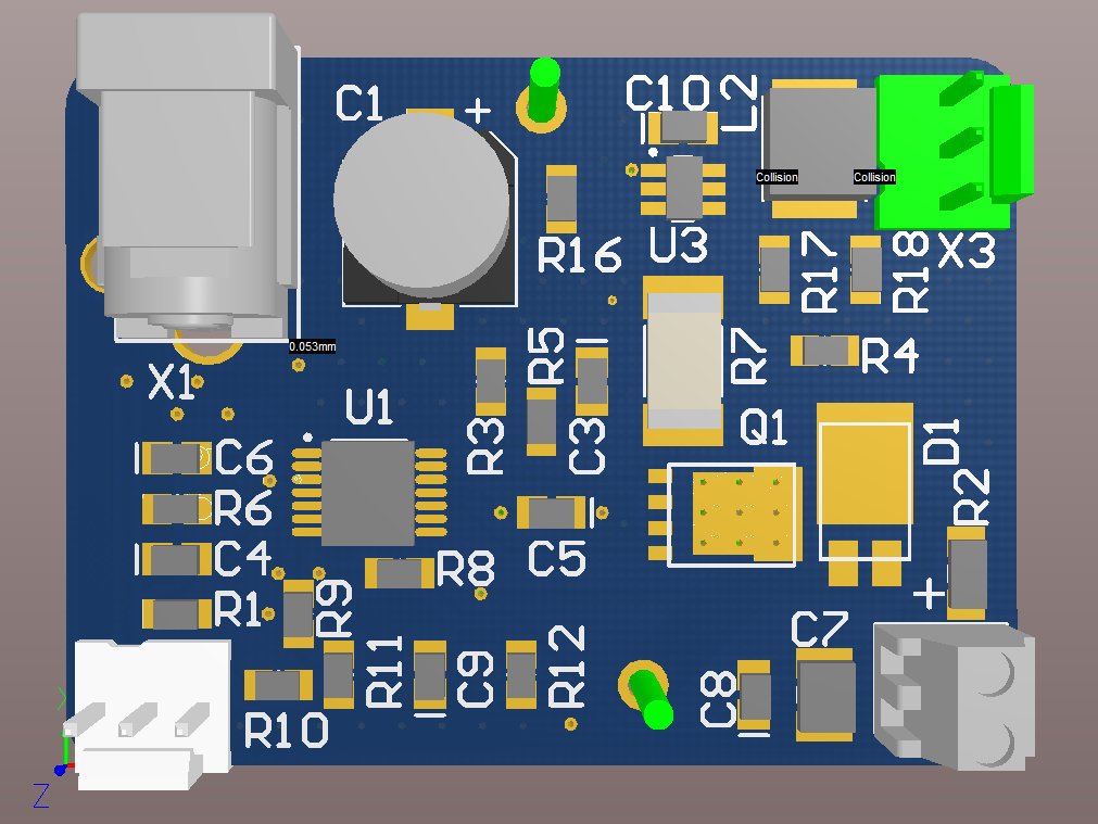
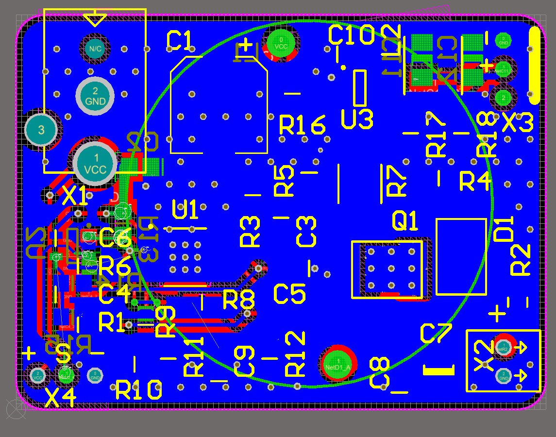
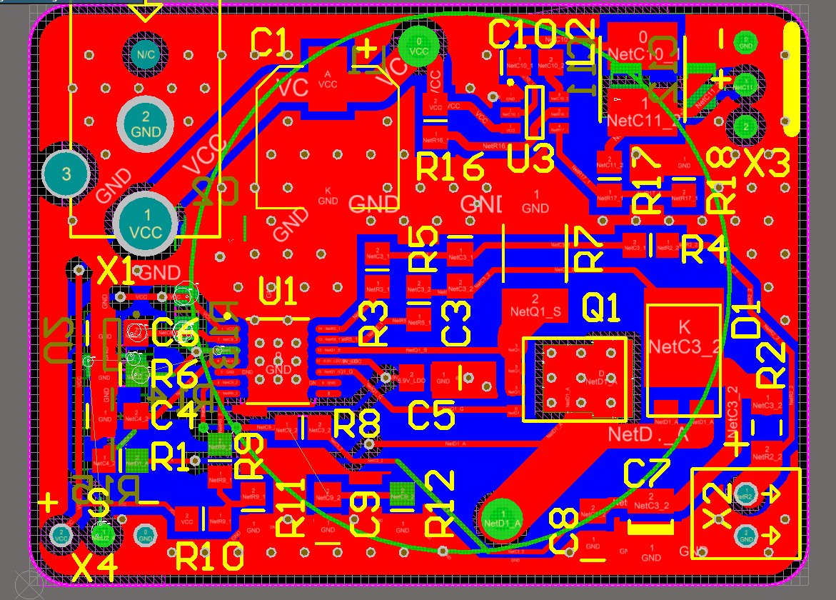
I would like to get some feedback on my PCB design, a critique if you will. This design uses the LM3429, as well as the TPS54202 for fan power.
In particular I would like to get an idea if this board is "Good, Bad, or Ugly". I've tried to minimize the current path from Q1/D1/R7 etc to as short as I can and have a big ground plane. with plenty of via stitching.
Output is ~1.1A at 60v with input being 19V at ~3.5A
This board will be the second revision, the first works OK but needed a couple tweaks, mainly a bit more heat sinking on Q1 (thermal vias added), as well as fixing a couple errors with the ground pour that causes some EMI issues. So ultimately I am just looking for some feedback to get an idea of how my layout skills are comparatively to what is expected in a professional setting.
Thanks!


