This thread has been locked.

If you have a related question, please click the "Ask a related question" button in the top right corner. The newly created question will be automatically linked to this question.

BQ24650: Boards wont work reliably when PCB assembled.

Part Number: BQ24650
Other Parts Discussed in Thread: CSD87350Q5D

Hi,


We are on our third board spin using the BQ24650 and we just can’t seem to get them to work reliably.


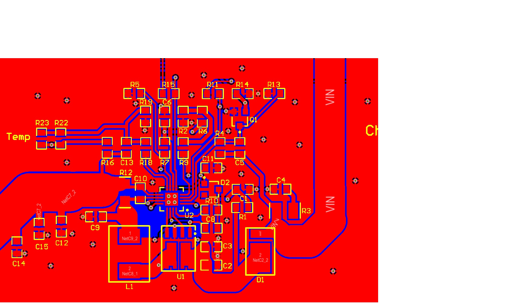
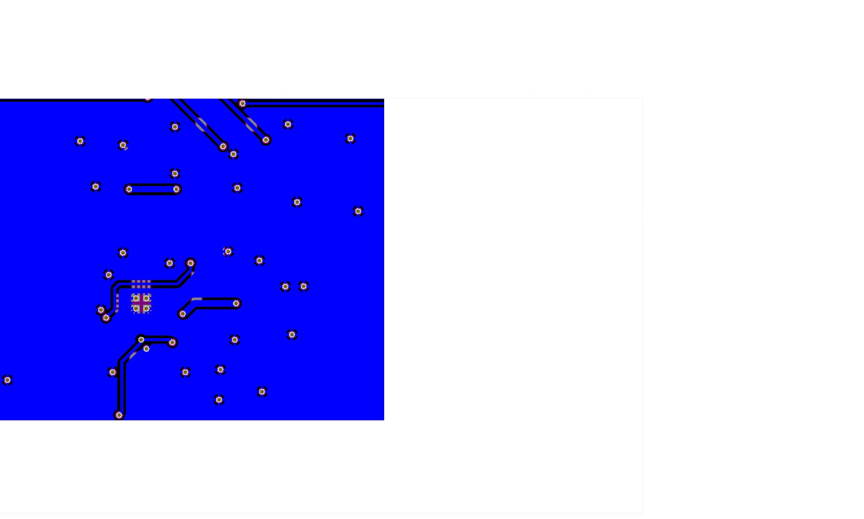
Our design is essentially the eval board setup for a 12v SLA battery.


We have built 20 of these boards in 3 different batches and only two have worked. The two that work are working well.  The ones that don’t work we cannot seem to fix.  We changed the QFN footprint twice, but we have also used the recommended footprint from the Altium Vault for this part.


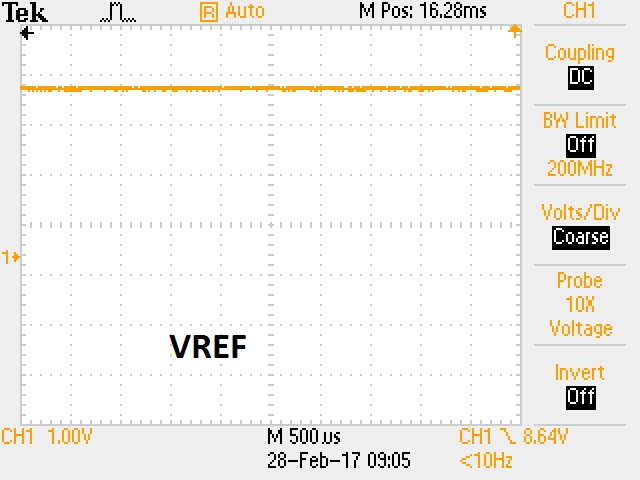
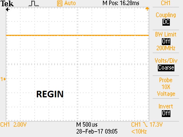
When they don’t work the charge light is on but there is no output from the switcher and the FET drive pins are not doing anything.


It seems like something is marginal but we can’t find it despite some major effort of some senior guys.


This solar charger should be the simplest part of our project, but it is the only part that we can’t make work reliably. Any input would be appreciated. I enclosed the schematic (I think)..


Thanks,


Aaron

  • Hi Aaron,

    Let's get to the bottom of this. Please try to upload the schematic again. Also, share the board layout, could be something wrong with component placement creating problems on the sense signals. You will have to "use rich formatting" that is below the reply box and upload from there.

    Please provide voltmeter readings on VCC, SRN, VFB, REGN, VREF, MPPSET and TS.

    Also, send a scope screenshot of HIDRV, LODRV, PH, VREF and REGN. I want to see if there is any noise being caught by VREF and REGN. Also, I want to see if there is some problem on the drivers if they are even switching by a tiny bit or not at all.

    Try changing the IC from the working board to a bad board, see if the problem follows the IC or the board.

    Regards,
    Steven
  • Hi Steven,


    I will try to send you the schematic and layout again.  It pasted fine but did not appear in the forum.


    I have tried many ICs from both Mouser and Digikey and one off the TI eval board.  Same thing.  I have also done the layout two times.


    I will get the measurements after this post.


    Thanks,


    Aaron

  • Hi Steven,

    Unfortunately, production shipped all the board off to see if they could find any QFN issues. The couple boards I have here are working and I am on vacation tomorrow for ten days.

    I will pick this up when I return. If you don’t mind taking a quick look at the schematic I posted that would be great. It is a simple circuit. I am quite sure however that is all fine.

    Thanks!

    Aaron
  • Hi Seven,


    Sorry about the delay. I just got back yesterday.


    While I was gone we had the lady who builds boards by hand populate two more. They don’t work either.


    The failure is the same. As you bring the solar in voltage up from 0 to 20v, the charge LED comes on at about 8v. There is never any chnarge output voltage generated. The switcher does not operate.


    The below numbers and scope shots you requested were made with no battery connected and the input voltage of about 20.5vdc.


    VCC = 20v

    SRN = 70mv

    VFB = 10mv

    REGN = 5.8v

    MPPSET = 532mv

    TS = 1.94v


    Thanks,


    Aaron

  • Hi Aaron,

    I looked at both your schematic and layout. Here are my suggestions:
    On the schematic:
    1. Change C1 to 1uF
    2. Change R3 to 2ohm, C4 to 2.2uF
    3. Have at least 20uF close to the sense resistor at SRN for best stability

    On the layout:
    1. C9 is to be placed close to IC on the SRP trace, not next to the inductor
    2. The PH node routing is not optimal, we suggest to not use any vias for the power stage. I understand this is due to the FET configuration. I suggest using csd87350q5d as it is optimized for synchronous buck operation and layout.
    3. Output capacitance should be placed as close as possible to the sense resistor

    Also, I noticed that MPPSET is at ~500mV, which at this point will not allow the converter to start. MPPSET needs to be above 1.2V for the converter to start switching. Please check the resistor values, and also make sure that Q1 is not turned on.

    Regards,
    Steven
  • Hi Steven,

    Thanks for the feedback.  The one board had a bad on/off FET that keeping MPPSET below 1.2v.  However, with your advice and the new buck dual FET, my boards seem to be working much better.

    Aaron