This thread has been locked.

If you have a related question, please click the "Ask a related question" button in the top right corner. The newly created question will be automatically linked to this question.

BQ24170: automatically goes to charge disabled

Part Number: BQ24170

Hi there,

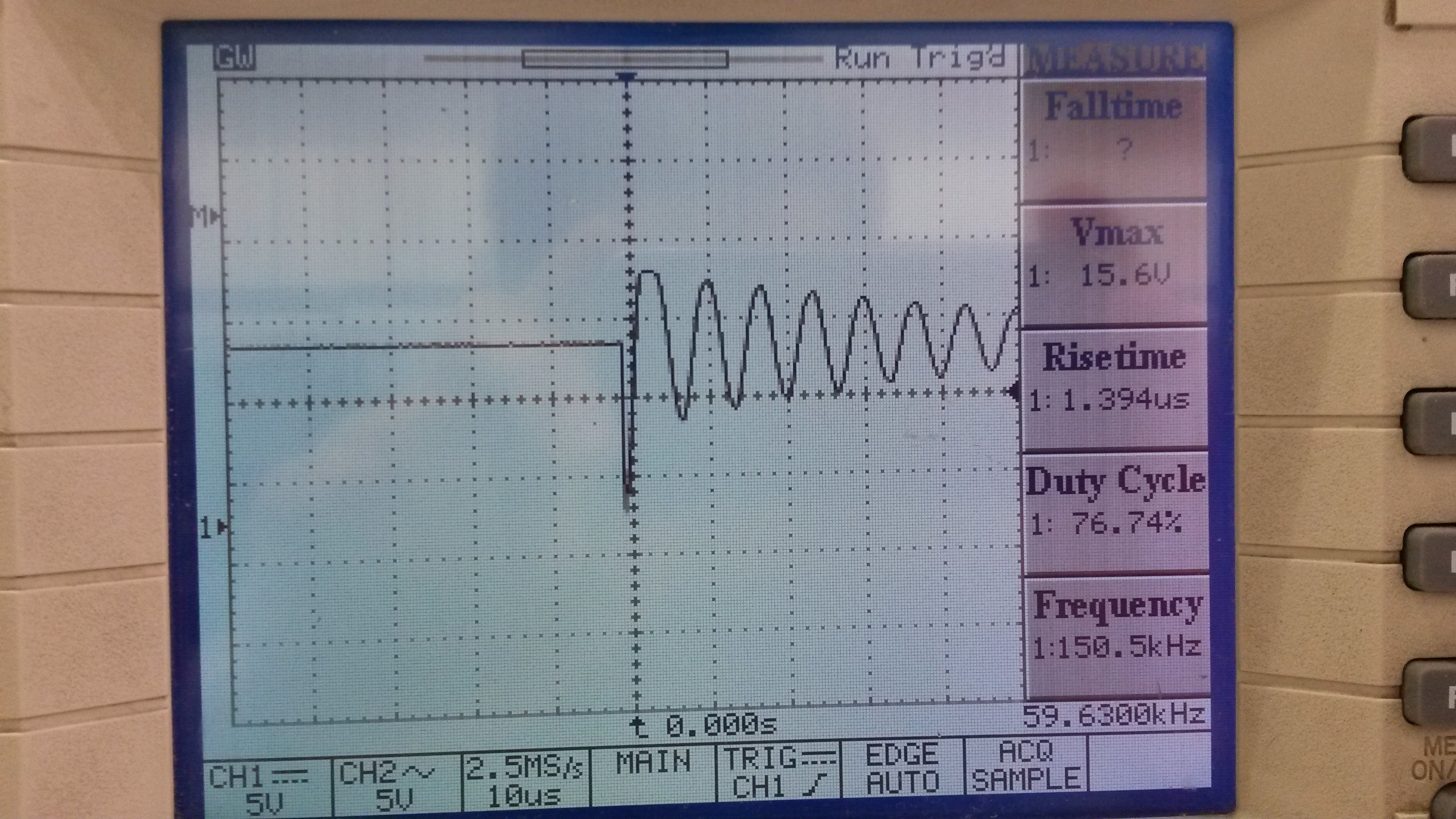
I'm triing to make a 3s2p li-ion charger, but it  simple go to charge disable according to the figure4 on page 13 on the datasheet (slusad2c). i am conecting in this order:

1.-connect the battery

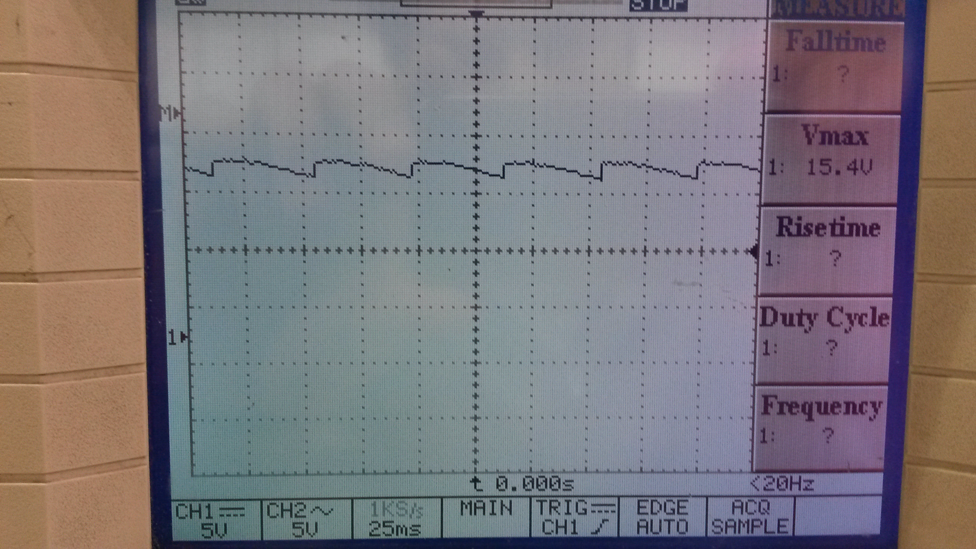
2.-conect the power supply(15.4 vdc),

3.- aprox 2 second Vin is conected, status pin is low(this drives a led on), and at the same time i get the signal on SW, same as the figure 4 page 13 on datasheet (slusad2c)

additional information:

Vin=15.4V

nominal cell voltage= 3.7v

full charge cell voltage=4.2v

capacity per cell = 650mah

total capacity= 6*650mah= 3900mAh

Vbat=11.5 (voltage on a series of 3 cells,test of charging starts at this voltage)

Vref=3.298V

Viset= .400v(this sets fast charge at 2amp)

Vacset= .600v(this sets input current limit to 3amp)

Icharge= -.005amp

Vregn=6.00v

cell pin= 3.3v(conected to vref with  1kohm resistor)

power supply is able to source 3 amps.(tested directly to another battery without any charger)

pvcc= 15v


  • I couldn't see any figures. Can you upload again.
  • Ok lets see know, i attached a powerpoint file indicating where im meassuring with an osciloscope, and the diagram that im following, hope this can clarify the problem.

    bq24170 problems.pptx

  • The setup con CELL pin is for 3 Cells not 4. Sorry
  • It looks like a Layout problem. Can you provide your schmatic, Layout and plot the SW, SRN, IL, PVCC waveforms?
  • Here is my shcematic and my board files,

    Note.- im using one layer board , made in house, with a cnc router machine.

  • Hi.
    It seems layout problems.You should layout by hand and follow Layout Guidelines(the Page 31 of the datasheet ) below:

    12.1 Layout Guidelines
    The switching node rise and fall times should be minimized for minimum switching loss. Proper layout of the
    components to minimize high-frequency current-path loop (see Figure 23) is important to prevent electrical and
    magnetic field radiation and high-frequency resonant problems. Here is a PCB layout priority list for proper
    layout. Layout of the PCB according to this specific order is essential.
    1. Place the input capacitor as close as possible to switching MOSFET supply and ground connections and use
    the shortest possible copper trace connection. These parts should be placed on the same layer of the PCB
    instead of on different layers and using vias to make this connection.
    2. The IC should be placed close to the switching MOSFET gate terminals to keep the gate-drive signal traces
    short for a clean MOSFET drive. The IC can be placed on the other side of the PCB from the switching
    MOSFETs.
    3. Place the inductor input terminal as close as possible to the switching MOSFET output terminal. Minimize the
    copper area of this trace to lower electrical and magnetic field radiation, but make the trace wide enough to
    carry the charging current. Do not use multiple layers in parallel for this connection. Minimize parasitic
    capacitance from this area to any other trace or plane.
    4. The charging-current sensing resistor should be placed right next to the inductor output. Route the sense
    leads connected across the sensing resistor back to the IC in same layer, close to each other (minimize loop
    area) and do not route the sense leads through a high-current path (see Figure 24 for Kelvin connection for
    best current accuracy). Place the decoupling capacitor on these traces next to the IC.
    5. Place the output capacitor next to the sensing resistor output and ground.
    6. Output capacitor ground connections must be tied to the same copper that connects to the input capacitor
    ground before connecting to system ground.
    7. Route the analog ground separately from the power ground and use a single ground connection to tie the
    charger power ground to the charger analog ground. Just beneath the IC, use the copper-pour for analog
    ground, but avoid power pins to reduce inductive and capacitive noise coupling. Connect analog ground to
    GND. Connect analog ground and power ground together using the thermal pad as the single ground
    connection point. Or use a 0-Ω resistor to tie analog ground to power ground (thermal pad should tie to
    analog ground in this case). A star connection under the thermal pad is highly recommended.
    8. It is critical to solder the exposed thermal pad on the back side of the IC package to the PCB ground. Ensure
    that there are sufficient thermal vias directly under the IC, connecting to the ground plane on the other layers.
    9. Place decoupling capacitors next to the IC pins and make trace connection as short as possible.
    10. Size and number of all vias must be enough for a given current path.
    See the EVM design (SLUU396) for the recommended component placement with trace and via locations.
  • SW WAVEFORM:


    SRN WAVEFORM:


    PVCC WAVEFORM:


    And this signal is looks weird for me: 

    ACDRV: