This thread has been locked.

If you have a related question, please click the "Ask a related question" button in the top right corner. The newly created question will be automatically linked to this question.

TPS55340: Stability of the frequency / Duty cycle

Part Number: TPS55340
Other Parts Discussed in Thread: , TPS40200

Dear,

I've got some issue to make the TPS55340 working properly.

Need to create a 18V continuous based on a 15V +/-10% for a load of lower than 1A => step of about 1A for a dv lower than 0.5V.

I use the excel file to define the value of the component to use for the compensation.

I try many different compensations solution but I have always the same behavior:

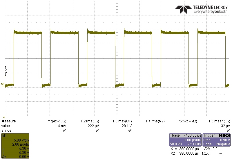
For instance, at 14V, I've this when I lood to SW pins of the component: (stable and almost constant => under 20OHm load)

When I increase the input voltage the duty cycle start to oscillate and the frequency seems to change. On the table it seems to work but as soon as I place it in our product and under temperature after short time under high load the regulation stop completely working (I got lower than 15V instead of 18V). I need to switch OFF and ON to make it work again ....

Do you know what is the root cause of this issue ?


Thanks.

Best Regards,

  • hi Fabien,

    we need to examine your schematic, but on the spot I dread you are triggering the maximum duty-cycle limitation (89%) of the device...

    you can verify this with a simple test:
    - starts from 12-13V in, 18Vout @ no current...
    - slowly increase the current up to the nominal load 1A (up to this point everything should be fine)
    - slowly increase the VIN up to the point you see the "strange behaviour"
    - at this point reduce the load and the "behaviour" will disappear

    if this happens, then my guess is correct (without looking at the design)
    hoep this helped a bit
    KR
    Vincenzo

  • Hello Vincenzo,

    I'm made my schematic based on WEBENCH first.

    But with this I was not able to load it to get 1 A.

    I update it by reducing the frequency to 400kHz and it seems to works on my desk but I saw that the heating of L1 and D1 was to much for our application so I modified them (take bigger ones)

    Then I try to follow the excel sheet and try many different compensations with different target crossover frequency. It has an impact but I steel don't get a stable product from 14V to 16V ...

    On the table with a fix load it was "working" (I was not able to make the regulation stop) but after when I place it into our product where the load vary, then after some time it stop regulating. (it was not necesseraly during a load modificaiton but could not maintain the highest current during a long moment)

    I try also to increase the output capacitance and everytime updating the compensation. Also changing switching frequency and Coil value.

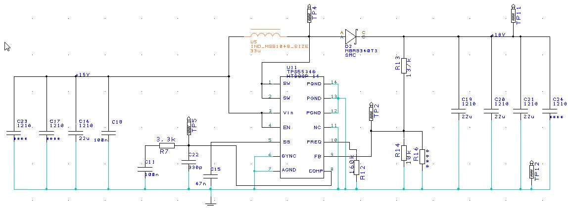
    Here is my last trial made:

    Regarding your comment it's what I see. Even from 14 to 16V with a load load is okay, it's when I place the high load that the behavior appear. Depending of the compensation it could be "stable" from 15 to 16 and not below and the contrary ... But it's always stable with a lower load.

    Regarding the duty cycle, based on the calculation It should be far away from the limit => Calculation said Dmin 14% and Dmax 24% ....

    Could I make it work if it's a duty cycle limitation ? If yes can you explain then why ?


    Thanks.

    Best Regards,

    Fabien.

  • hi Fabien,

    yes also from the waveforms is not the duty limitation...

    spreadsheet and webench are reliable enough, so ... are you sure the actual load is not too high?

    have you used the EVM for the test? just to remove also the layout from the equation ...

    use this bom on EVM if possible (unfortunately I have no bandwidth to do the tests for you here)

    webench_design_1209005_528_15988062.pdf

    KR

    Vincenzo

  • Hello,

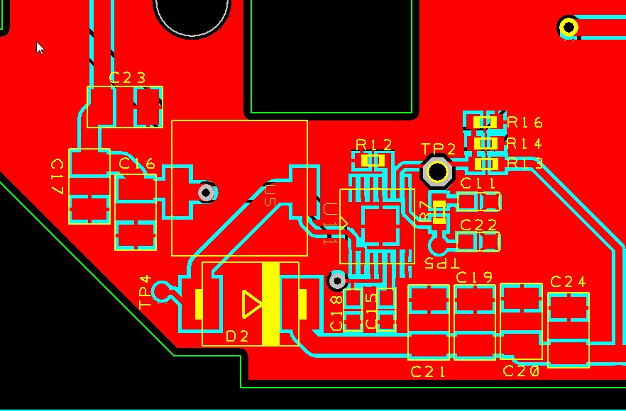
    Here is the layout.

    No I didn't try with a EVM ... +15V arrived on C23 and +18V should be on C24.

    Do you think is a layout issue ?

    I've try with another components: (follow your switcher pro selection ...)

    But it don't work at all ... I don't get 18V on the outside . I don't get why for the moment.

    I'm a bit frustrating to know that it works in my application but I'm not able to make the +18V working during high load condition ...

    Any clue to solve my issue with the TPS55340. I will try this afternoon your proposal but I don't have a 5.6uH coil ... only 8.2uH ...

    Let's see.

    Best Regards

  • hi Fabien,

    I'm very sorry to tell you that with this layout you can't go anywhere  :(

    there are a lot of weakness, the worst one is the path from the inductor / diode node to the drain of the booster FET: this you routed as a normal signal trace, introducing a very high Z that affects the system perfomance...

    please see the comparison of the trace I mentioned w/ the EVM layout:

    I would recommend you to get an EVM, validate the bom and then re-do the layout in according to the guidelines...

    feel free to submit it here for a check

    KR

    Vincenzo

  • Hello,

    Thanks for your feedback.

    I've ordered a EVM to see if it will work in our case => TPS55340EVM-017

    In the meantime I've updated the layout. Do you think is it better ? Anyother comment or big mistake ?

    U13 is a Aluminium capacitor in case of ...

    Thanks.

    Best Regards,

  • hi Fabien,

    yes I have comments/feedback on that...

    I will be back to you asap...

    KR

    Vincenzo

  • hi Fabien,

    please find in attachment my comments plus a general guidelines for DC/DC switching converters

    if you have questions, just ask

    KR

    Vincenzo

    VP.docx

    Layout guideline.pptx

  • Hello,

    Many thanks for your comment.

    I will update according to your comments.

    I have only one question based on your comment is about:

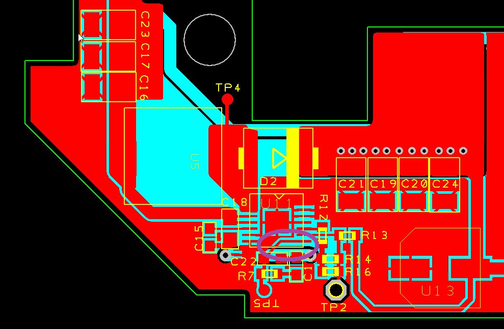
    " Don't route signals under the pad" => where ?

    I've made a 2 layers PCB. Could it be an issue?

    On the Bottom there there is no signal, except those:

    Thanks.
    Best Regards,

    Fabien

  • hi Fabien,

    I meant the trace I highlighted here:

    you can just flip 90degrees CW the block C22 / C11 / R7...

    4 layers would be better from noise point of view, but if the board is not super crowded and as long as you provide enough GND copper, two layers pcb is ok...

    please remove the thermal relief to the vias (the key points that connect the various GND lands)...

    KR

    Vincenzo

  • Hello Vincenzo,

    Thanks for your feedback.

    I was in Holidays this is why I didn't can back earlier.

    With the EVM that I'm buy I didn't get the issue I have earlier so as you said it seems that you were right.

    I will launch a new PCB prototype ASAP.

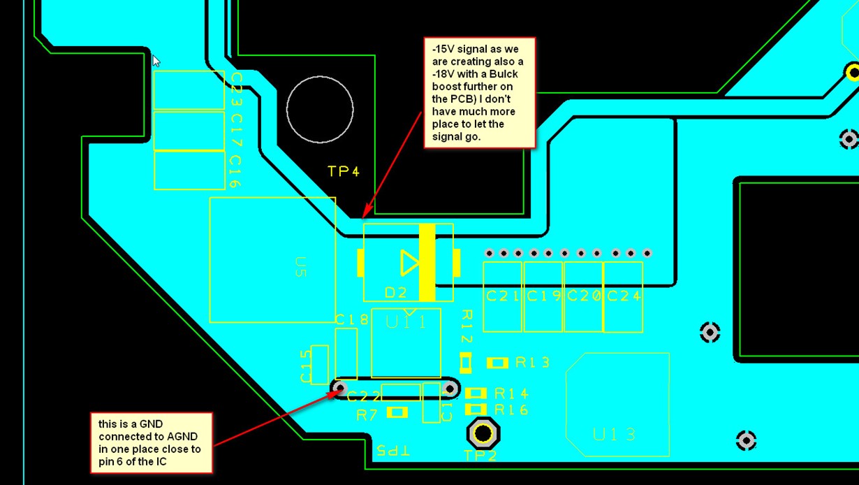
    I have another question which is on the same PCB.

    With the TPS55340, I'm making a +18V from a +15V.

    Further on the PCB I'm making a -18V from a -15V.

    Today it has worked as it was.

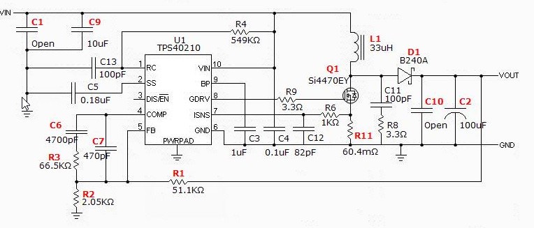
    Like this: (using a TPS40200 based on PMP4589)

    I want to improve the layout to this.

    Is it better?

    I try to follow the recommandation but as all are invert (the VDD is connected to the GND), I'm wondering If I'm doing right ...

    Your comment will be appreciated.

    Thanks.

    Best Regards,

    Fabien

  • Presentation1.pptxhi Fabien,

    please find my  comments in attachment...

    PS: I didn't see the feedback divider to/from VOUT (check the schematic!)  :)

    hope this helped a bit

    KR

    Vincenzo

  • I've made the recommanded modifications and it has worked.

    Thanks for your help!!

    Best Regards,
    Fabien