


Other Parts Discussed in Thread: UCC28700
Hello,
i'm designing an onboard charger, and came to the gounding confusion for the isolated gate driver for driving the UCC28951-Q1 signals.
In my application, I've implement the UCC28700 for bias flyback supply with isolated ground (Sec Bias Flyback). Upon drawing up the schematics, it seems like I am not allowed to use this supply to drive the MOSFET's gate. Otherwise high voltage ground will be joined with low-voltage ground through the MOSFET source pin.
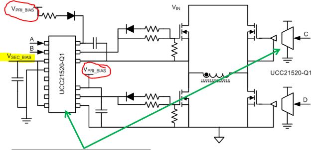
I have watched the TI training series "How to Design Multi-kW DC/DC Converters for Electric Vehicles (EVs) (part 4)" and on slide #35, it shows that the gate drivers were driven by 2 supplies (VSEC_BIAS + VPRI_BIAS).
Do i actually have to implement the same UCC28700 bias supply again with common ground (Pri Bias Flyback) and have doubled the component count? Am i understanding the concept correct?


