Hello,
Could you help to check below schematic and layout?
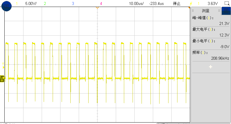
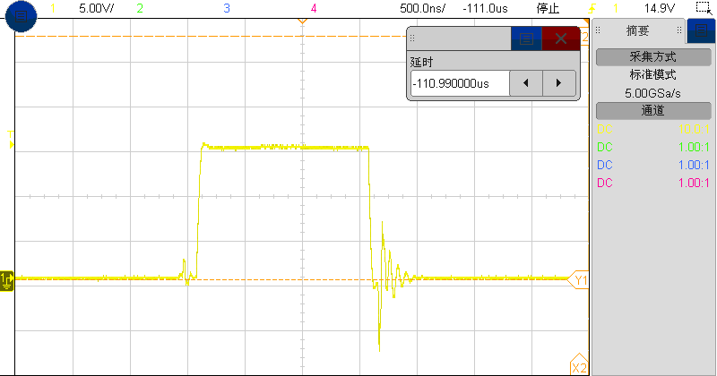
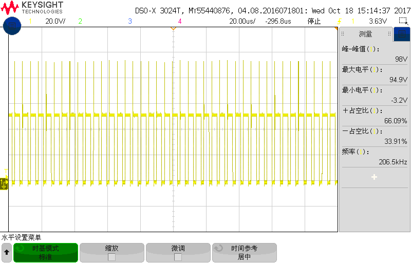
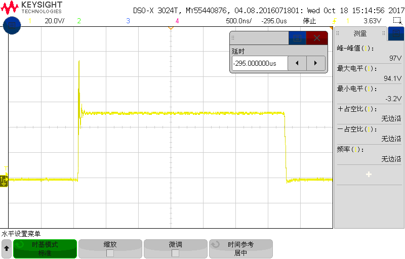
Input 54V-84V, output 36V 8A, switching frequency 200kHz.

Thanks and best regards,
Victor
Hello,
Could you help to check below schematic and layout?
Input 54V-84V, output 36V 8A, switching frequency 200kHz.
Thanks and best regards,
Victor