This thread has been locked.

If you have a related question, please click the "Ask a related question" button in the top right corner. The newly created question will be automatically linked to this question.

TPS53819A: The TPS53819 SW waveform question?

Part Number: TPS53819A
Other Parts Discussed in Thread: TPS53819

Hi Sir

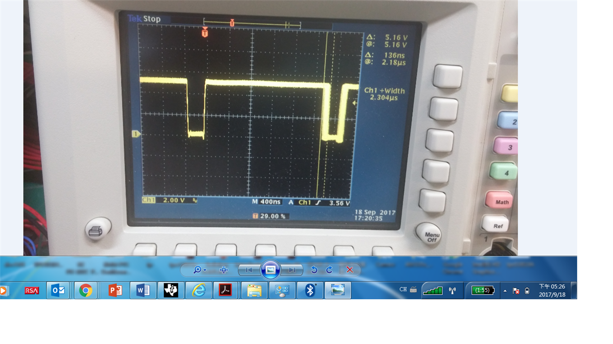
we go to measure customer TPS53819 SW waveform and find there have a little jitter in waveform.

I find the customer 2 point different, may i check if these 2 point will generate jitter in SW pin?

1. compare EVB and customer circuit, i find the EVB have spreate Digital GND and Analog GND. but customer have no.

2. The EVB is use CSD87350 and my customer use discrate MOS to replace.

Test condition is 12 Vin 1Vout 20A.

tpe53819a.pdf

  • Bogey,

    Are you sure this is the SW pin waveform. Vin=12V, Vo=1V is close to 10% duty cycle. The waveform shown here is having much higher duty cycle. Some amount of jitter at turn off is normal but you can compare the data with evm like you were doing.

    Regards,

    Mathew

  • Hi Mathew

    Is there have way to reduce jitter? and if there having document to description  this kind control way?

                                                          Bogey

  • Bogey,
    The schematic looks okay. Please check Vin ripple (ac coupled) to see the ripple. I would recommend adding more ceramic caps to the input,
    If the output curent is 25A or so would recommend adding 4 more 10uF. This keep the ripple current within limits for caps and reduce jitter also.

    Regards,
    Mathew