This thread has been locked.

If you have a related question, please click the "Ask a related question" button in the top right corner. The newly created question will be automatically linked to this question.

TPS65131: Negative supply does not ramp up under load condition

Part Number: TPS65131
Other Parts Discussed in Thread: TPS65130

Hello,

I am currently trying to TPS65131 for an audio project. My requirements are:

* single LiPo Cell source

* +/- 12V output

* up to 100mA per side

* no noise in the audio band

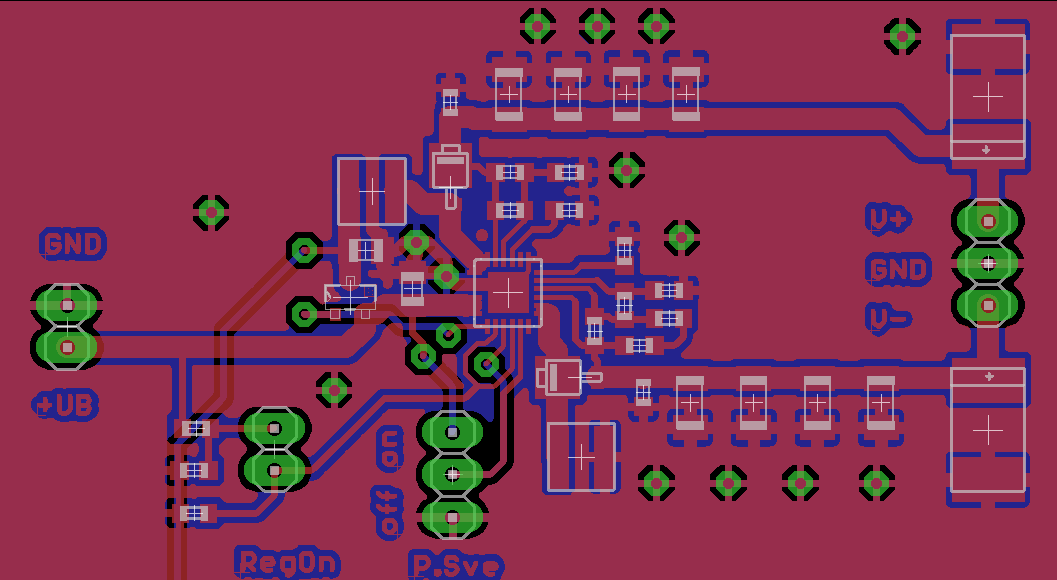
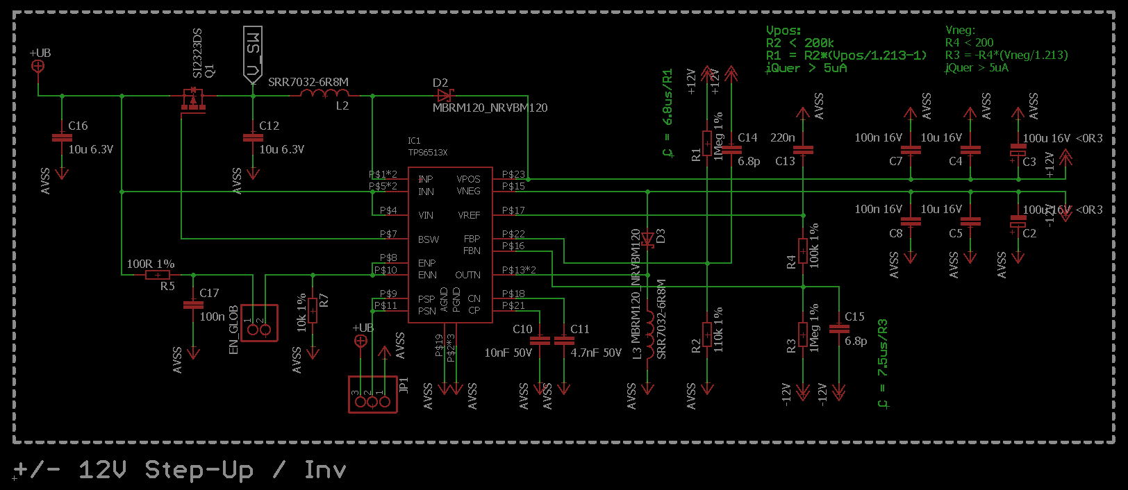
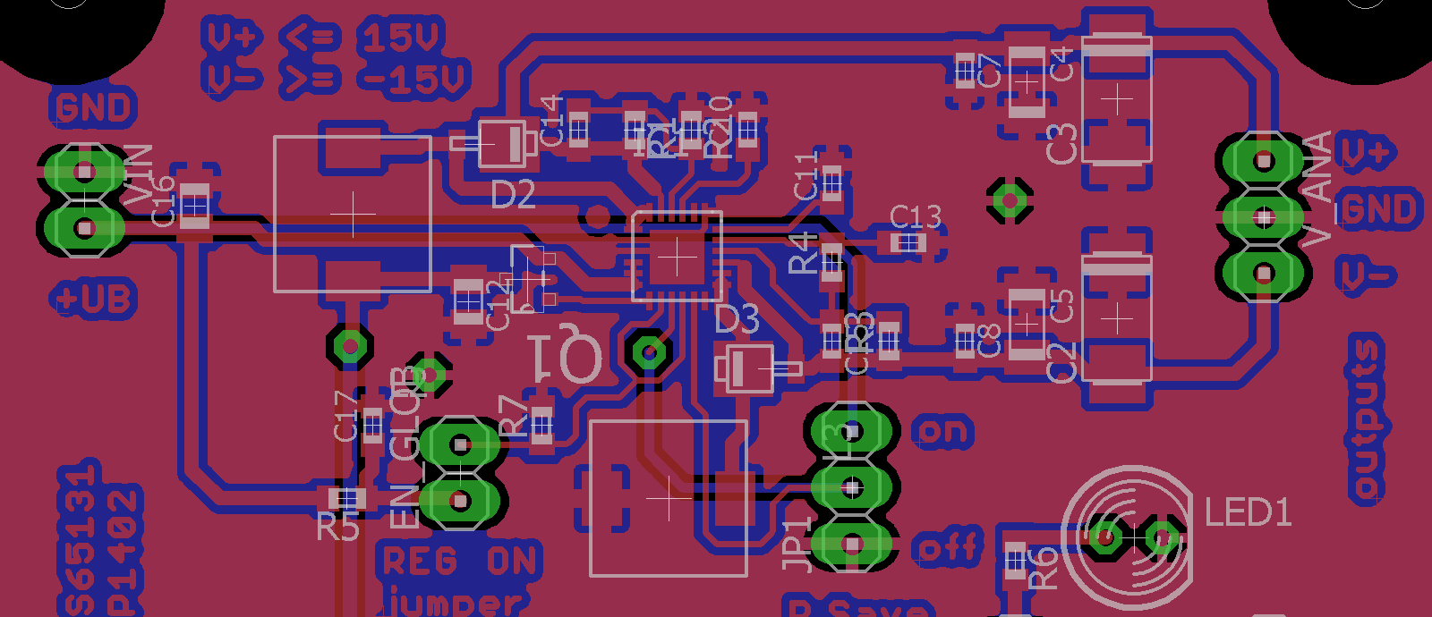
For Reference, my scematic and Layout:
(please note: the 100u tantal caps are not present at the moment. The 10u caps are 22u ceramic types at the moment)

The following is true:

* +12V works as desired in all below described screnarios

* with no load and power-safe on, -12V ramps up and stays relatively steady at -12V

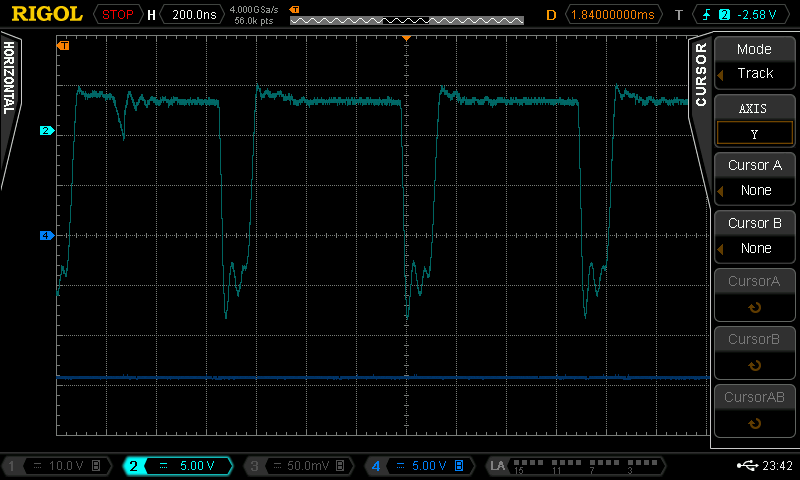
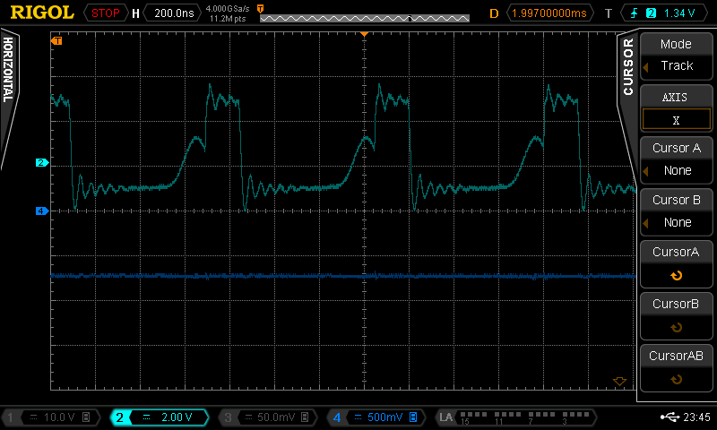
* with no load and power-safe off, -12V ramps up, but produces large 5V jumps in a sawetooth-manner

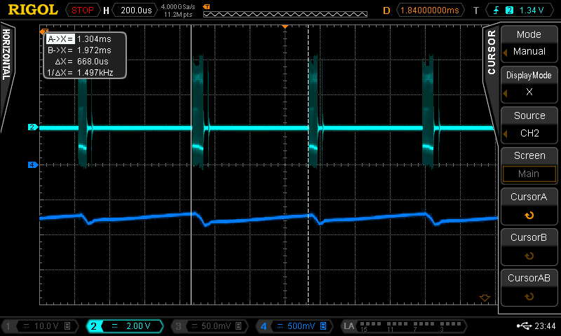
* with about 50mA Load and power-safe on, -12V fails to ramp up (sticks at ~ -0.2..-0.3V) and ~1..2 kHz noise is audible

* with about 50mA Load and power-safe on, -12V fails to ramp uo and ~1..2 kHz noise is audible

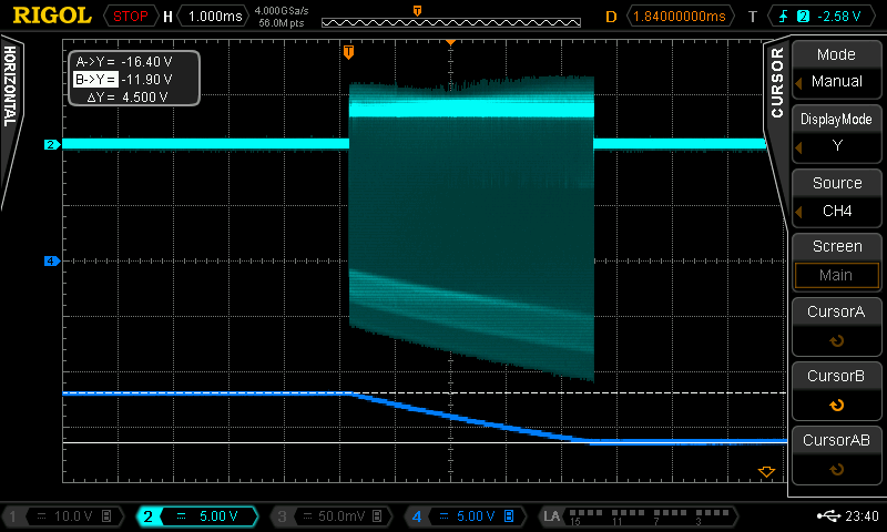
Here a Scope-Shot from one failed ramp-up attempt. The blue curve is the failed attempt.

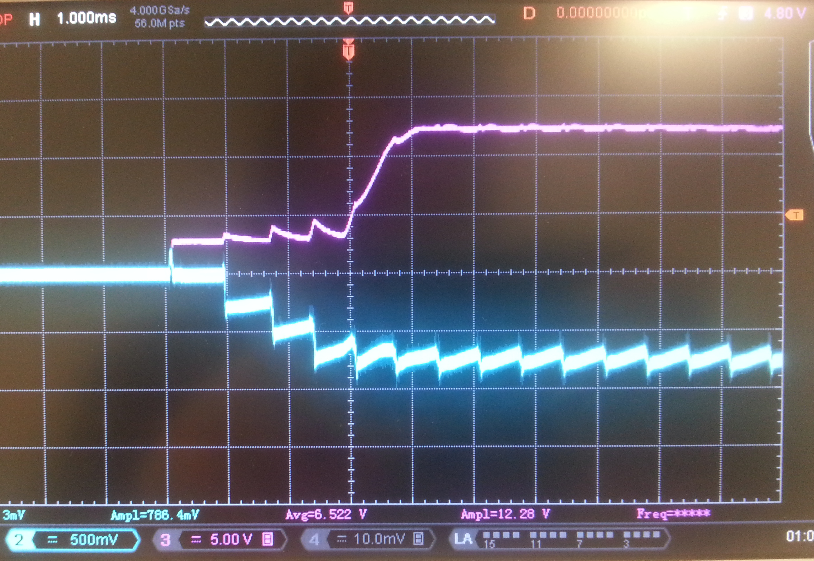
Measured under load Condition:

FBN: 1.064V (injected noise present)
VREF: 1.215 (injected noise present)
OUTN: -750mV (sawtooth, as shown above)

Ground potential is virtually the same on the board (in the range of 1..2 mV) and does however exhibit injected noise (then again, only a  couple of 10mV)

The following threads have already been consulted:


https://e2e.ti.com/support/power_management/non-isolated_dcdc/f/196/t/626451

https://e2e.ti.com/support/power_management/non-isolated_dcdc/f/196/t/607104

https://e2e.ti.com/support/power_management/non-isolated_dcdc/f/196/t/617831

https://e2e.ti.com/support/power_management/non-isolated_dcdc/f/196/t/585589


The following was tried:

* removing C15 (still does not ramp up)

* increasing C15 to 20p (still does not ramp up)

* using 6.8p and 100k in series instead of C15 alone (decreases no-load fluctuation amplitude significantly, but still no ramp-up)

The question is:

Why does the negative converter does not ramp up under load? Wham am i missing here?

Thank you a lot for help !

Kind regards

  • Me again,

    i took the time and did some screenshots from the start-up process of the step-up and inverting part seperately in all 4 configurations each.

    Below you will first find 4 pictures of the step-up part:

    ch1: GND
    ch2: FBP
    ch3: CP
    ch4: V+

    Pic1: no load, no power save
    Pic2: no load, power save
    Pic3: load, no power save
    Pic4: load, power save


    Here you find 4 pictures of the inverter part:

    ch1: VREF
    ch2: FBN
    ch3: CN
    ch4: V-

    1: no load, no power Save
    2: no load, power save
    3: load, no power save
    4: load, power save


    Please consider:

    * The inverting part does need a considerable longer start-up time

    * the last 2 pictures of the inverting part have a much different scaling in the channel 4 (V-). The final voltage is about -0.3 to -0.5V instead of -12V

    * supply voltage was 3V with 1.5A current limit

    * load was 220R

    * still, the inverting part only operates at no load 

    I would be thankful for any possible help.

    Kind regards

  • Hello Michael,

    Sure we will have a look at this asap.

    Best Regards.
    Ilona
  • Hello Ilona,

    I am looking forward to that. Thank you for letting me know, that I am not alone. In the meantime i have more scope shots for you, this time of the voltage across L3 (the inverting regulator inductor) with respect to ground.

    For all pictures is true:

    * no power save
    * 1st graph = voltage across inductor
    * 2nd graph = v- output voltage

    The following pictures show:

    1 - no load, single burst (burst are far apart)
    2 - no load, zoomed into burst

    3 - load, sequence of bursts
    4 - load, zoomed into burst

    Please note the following:

    * in no load config, the regulator bursts to -16.4V and then lets discharge the cap, to -11.9V, which is (abut) the target value of -12V, then bursts up again to -16.4V

    * in no load config, the bursts are FAR apart

    * in load config, the bursts are much higher frequented (~1.5kHz)

    * in load config, the bursts are much smaller in implitude (~6Vptp compared to ~ 20V and above in no load config)

    * the +12V rail also exhibits 1.5kHz bursting

    Please consider

    * -16.4V will damage my equiptment, thus this behaviour should be avoided

    * 1.5kHz bursts will be audible in my audio application, how to avoid that for both rails? (for later, when everythingelse works fine)

    * and of curse, the -12V is at about -500mV, that is the main problem at hand ; )

    kind regards

  • Hello,

    still no clue what might went wrong? I am starting to run out of options over here..

    Kind regards

  • Hello,

    still in the dark over here, has anybody any idea what might cause this problem?

    Kind regards
  • Hello Michael,

    Please excuse the late response to your problem. It sounds as if you have a layout issue.
    I expect high noise injection into the AGND because you connected the output caps directly to the AGND, but the path to the PGND pins is really long. Please check out the layout of the EVM and the layout recommendations in the datasheet for updating the layout.
    On this part the CN, CP and VREF pins are somewhat sensitive to noise injection, but proper layout is essential for any switching power supply.
    In your layout, I think there are ground issues. In a switch mode power supply, GND is not just a reference potential but a signal that has to be routed as a signal and not just float the board with it.

    Especially the loops with alternating current/ voltage need to be laid out with care. In this case the following loops are most important:
    positive converter: diode -> output capacitor -> GND connection of output cap -> PGND pins of the IC -> INP pin -> diode
    negative converter: 1. input cap -> INN pins -> inductor -> GND connection of the input cap -> input cap
    2. OUTN pin -> inductor -> GND connection of the output cap -> output cap -> diode -> OUTN pin

    If you check these loops on your layout, you will see that these are really long which causes a lot of noise and most probable the issue your observe.

    Best regards,
    Brigitte
  • Dear Brigitte,

    thank you for your answer. I am of course well aware of the implications when routing a high current, high frequency lines. However, I was not aware of the particular high sensitivity in the TPS65131. Thank you for pointing that out.

    I am currently in the process of designing another layout. Due to process limitations I am somewhat limited in VIA placement which does not ease the design. I will report back if the new design arrives.

    Kind regards
  • Hello Michael,

    Do you have any update for us?

    Thanks.
    Best Regards.
    Ilona
  • Deart Ilona,

    indeed, I do. After careful redesigning the Layout (which was quiet a pain due to mentioned technological restrictions) I can say: it works. In addition I connected 3 parralel 10uF caps with a 100nF to each output in order to reduce overall ESR and lowered the coil inductance to 4.7uF. 

    In power save mode with approx. 56mA load (~223R load at +/- 12.4V) I get a ripple of 164mV at the +12V, 103mV at the -12V rail with a frequency of about 20kHz and an overall power drawn from the primary (3.0V) side of approx. 628mA. So i have approx. 74% Efficiency. 

    If power save mode is disabled, the power drawn increases only slightly to ~632mA and there is close to no measurable ripple, only neglectable high frequency noise in the 10mV range. This configuration leaves me with 73% efficiency.

    Regarding stability, noise and ripple I am quiet happy now. Only the efficiency could be a good 10% higher. Diodes are MBRM120, inductors are 4.7uF, 1.6A DC max, 150mOhm DC. Do you think I should invest in lower resistance inductors or even higher-current Schottkys to tackle the efficiency?

    Thank you a lot for your help and kind regards

  • Hello Michael,

    Thanks for your feedback, this is very valuable for us! Could you for comparison share with us the new layout ?
    In terms of the efficiency I do not see that much improvement opportunity here as the output current is just at the edge where it goes from PFM to forced PWM and does not effect the efficiency that much.
    What you still can try is to use a higher inductance (6.8µH) that will lower the output current ripple and thereby the DCR losses. As well check a bigger inductor (in terms of size) that reduces the DCR. I think your shottky is quite good, the forward voltage drop is at 300 mV at this condition...this is already quite low but of course you can try to exchange this with a higher-current one.

    Best Regards.
    ilona

  • Hello Ilona,

    of course, here is my new layout:

    Based on the datasheet I should be able to get at least about 80%+ efficiency in the current configuration. Or do the curves in Figure 12,14 and 18,20 respectively in [1] does only refer to the device itself without any external losses such as Inductors etc.?

    Kind regards

    [1] www.ti.com/.../tps65131.pdf

  • Hello MIchael,

    The efficiency data of course refers to measurements done on the EVM meaning with external components. Initially you intended to have 73%+10% more efficiency, this is what commented.

    When I look at the curves in the datasheet the measurements show that for your configuration (+/12V, 3-4V, 60mA) the efficiency is in the range of 76% (forced PWM) or 78 to 80% (PFM), I do not see that this is going beyond 80%. As said you can check if you can get components with better ratings, this should improve it definitely.

    Best Regards.

    Ilona

  • Hello Ilona,

    the chart you are referencing refers to the TPS65130 which, I suppose, may have a larger Ron in the internal switch. I, however, am using the TPS65131 which, as can be seen in Fig. 12 and Fig. 14 for the positve rail and Fig. 18 and Fig 20 for the negative tail, should easily exceed the 80% Efficiency on total with an output voltage of +/-12V (which is not specifically given, but interpolated between the 10 and 15 rails it should be well above 80%).

    Coming from 73%, an increase of close to 10% should be achievable. However, as the device is now functional I have to work on other aspects of the project and may return to the efficiency issue later on. For the time being: thank your for your advice.

    Kind regards