A related question is a question created from another question. When the related question is created, it will be automatically linked to the original question.
If you have a related question, please click the "Ask a related question" button in the top right corner. The newly created question will be automatically linked to this question.
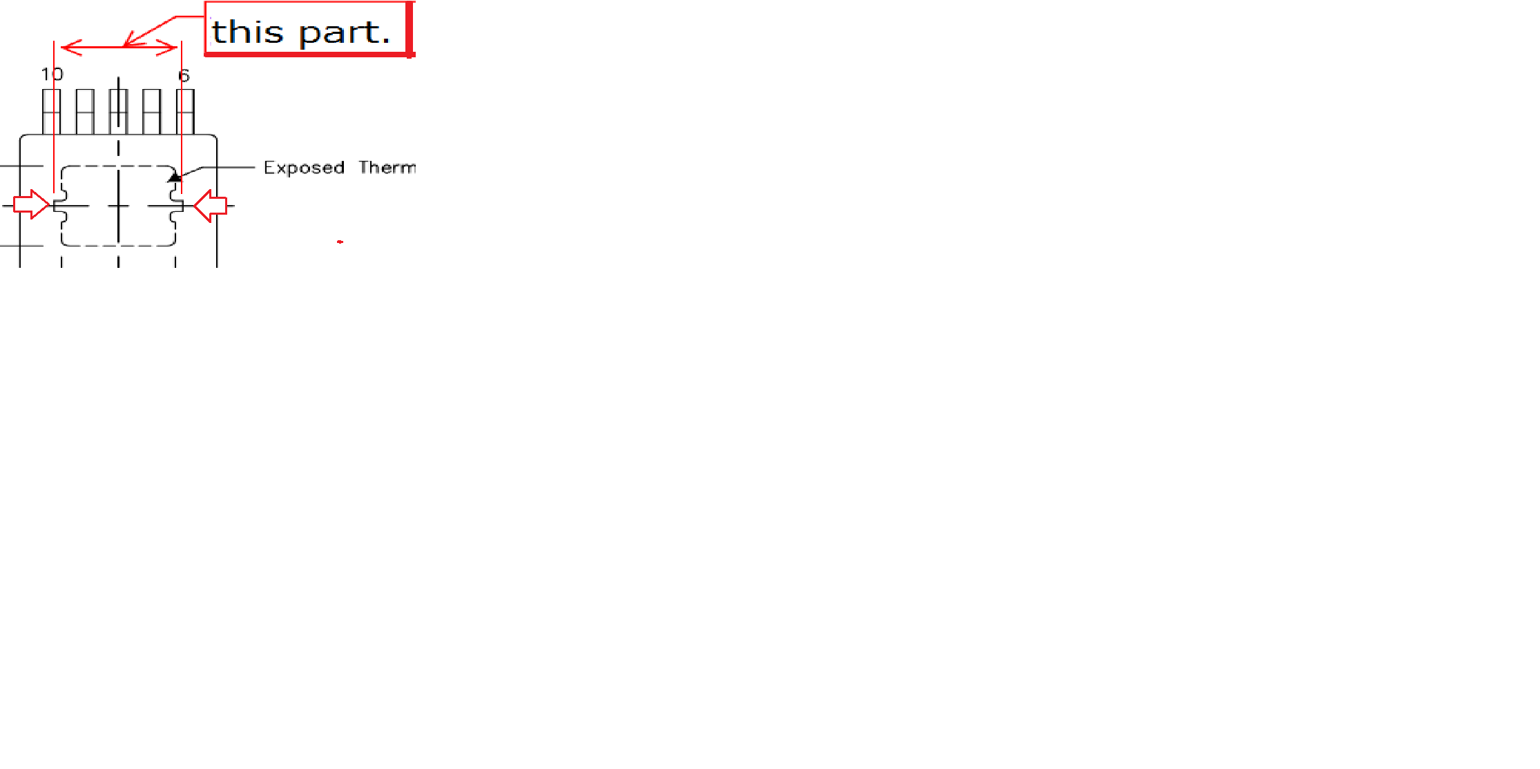
I cannot see any pictures attached, they are just little "x"s. In any case yes, those are the dimensions of the solder mask opening. See the datasheet section near the end titled "Thermal Pad Mechanical Data".
By the way, you can request the CAD symbol for this under the "Quality & Packaging" tab on the product page. All the dimensions will be the same as those we use for our EVMs.
The measurements on page 28 refer to the DAP of the IC with tolerances (min/max).
The measurements on page 29 are for the PCB land pattern which is the max DAP dimension in each direction so that all devices will solder down correctly.