Other Parts Discussed in Thread: , TPS61092
Hello TI,
Brief description:
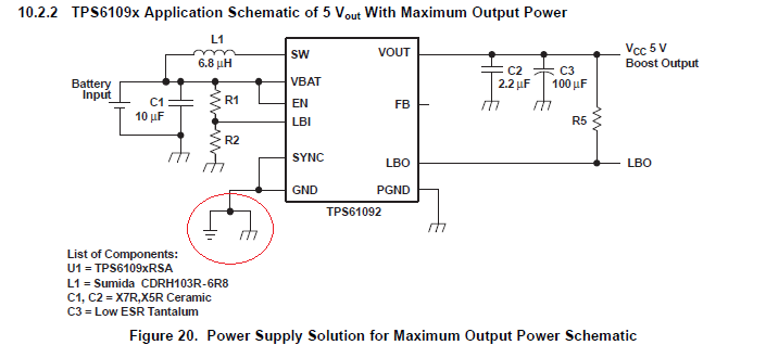
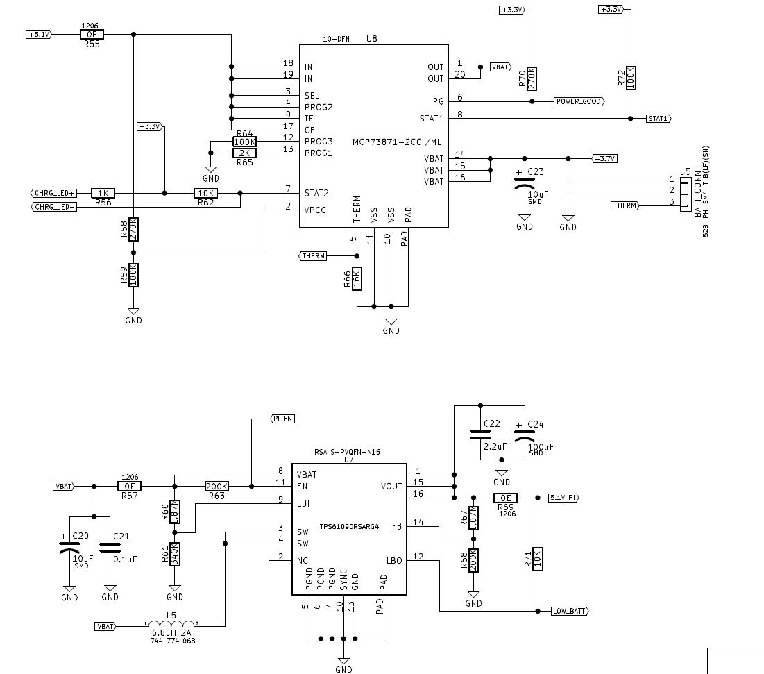
Our circuit contains 5V input adapter source given to MCP73871 (U8) charger IC with 3.7V Lithium Ion battery for backup. So during power fails battery takes in charge. This output is given to TPS61090RSARG4 (U7) IC which then boost the voltage to 5V and max load is only 500mA. I've attached our circuit diagram below including gerber view and placements. We have used these components for the first time in our designs and hoping to use it in future a lot.
Test Setup:
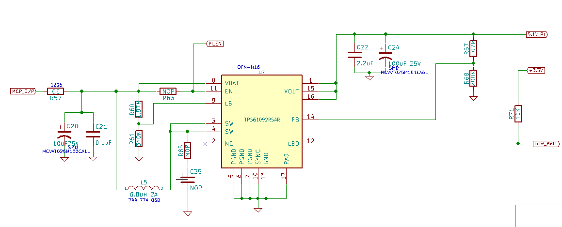
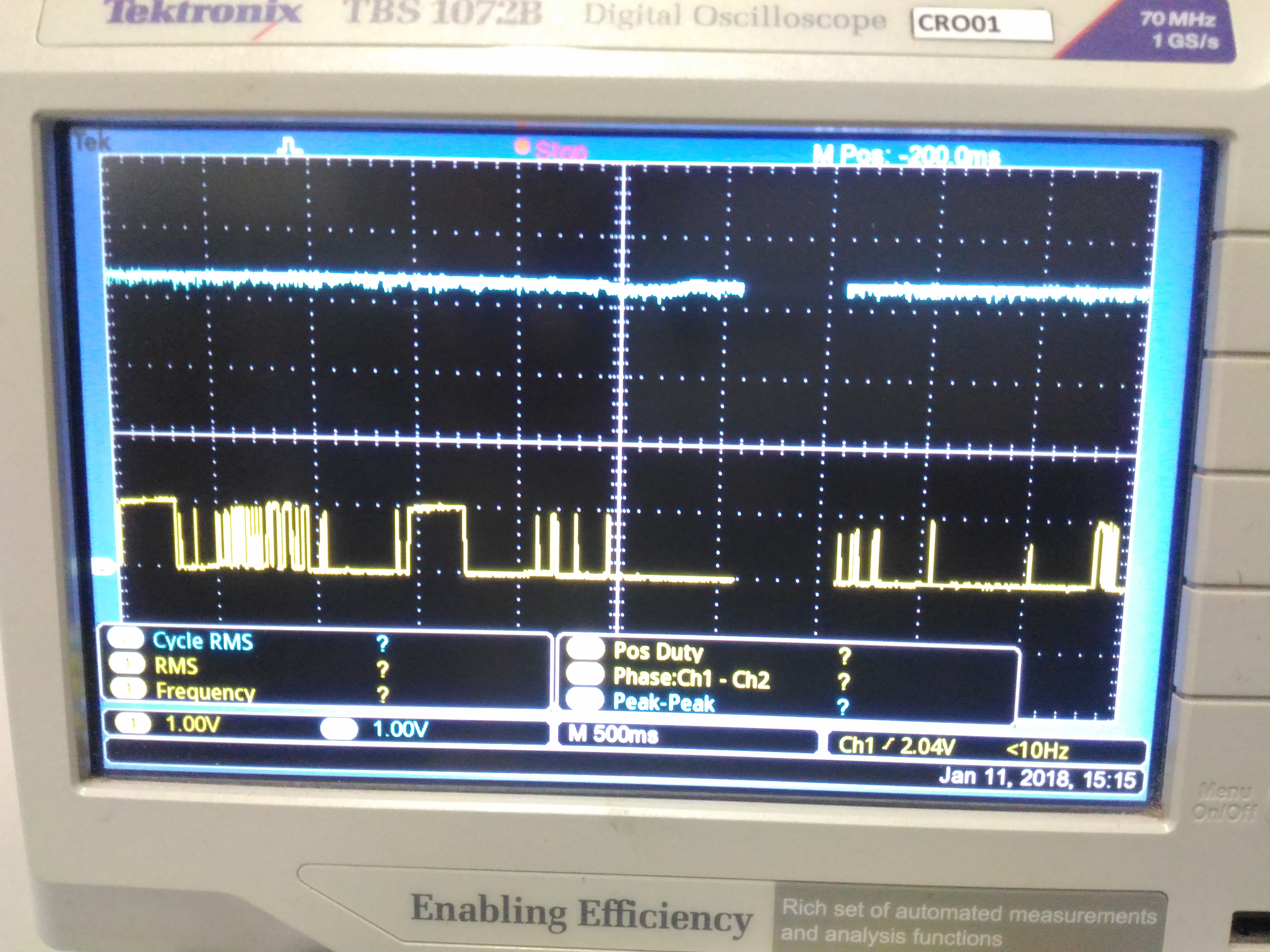
1. CRO Probe connected to TPS61090 VOUT at R69
2. Input voltage 5V Bench Supply given at R55 ( Not SMPS based) excluding rest of circuit with no LOAD's connected. (Input will be 7V 3A SMPS adapter in actual application)
3. Battery Not connected to charger circuit. (When battery is not connected the Input voltage at R55 is given as VBAT)
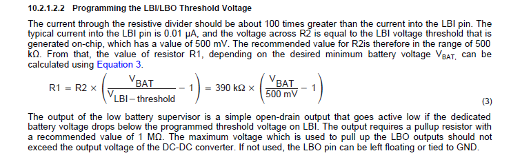
4. R67 = 1.8MOhms, R68= 200kOhms. (on CRO here it shows 0.540mV) (Correction done on Resistor divider)
5. The dot on 6.8uH power inductor is connected to VBAT,
6. PI_EN Pin is open in the circuit and going only to external connector.
Problem:
1. Circuit works fine for some time. Gives 5V output perfectly with no Load. After some time or sometimes immediately the TPS61090 IC gets short circuited pulling lot of current through Charger IC disabling output of Charger IC itself. So we put a 500mA PTC fuse which also doesn't help and still destroys the TPS61090 IC. CRO just shows low voltage at the output side and no way to debug what just happened.
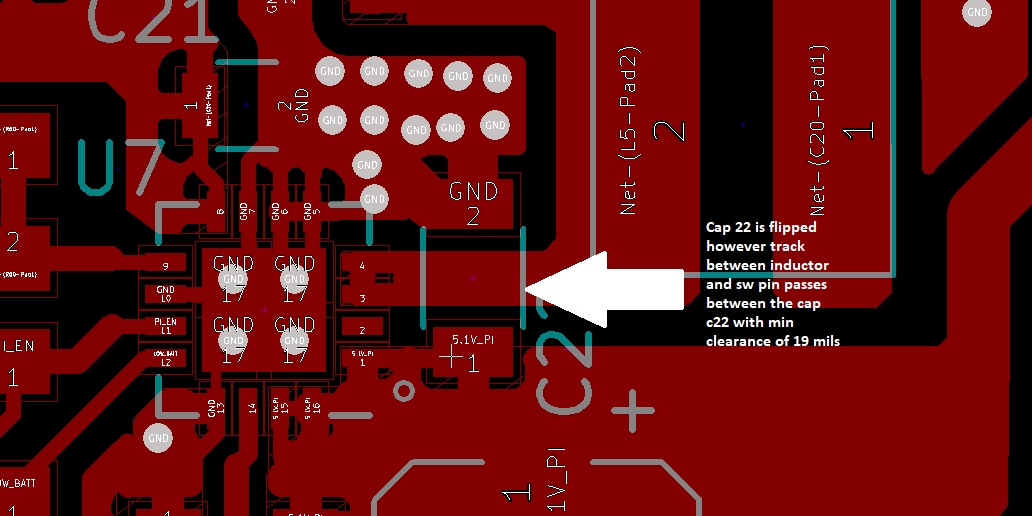
2. We have also noticed after removing the IC, pins 3,4 which is SW is getting shorted to PGND pins.
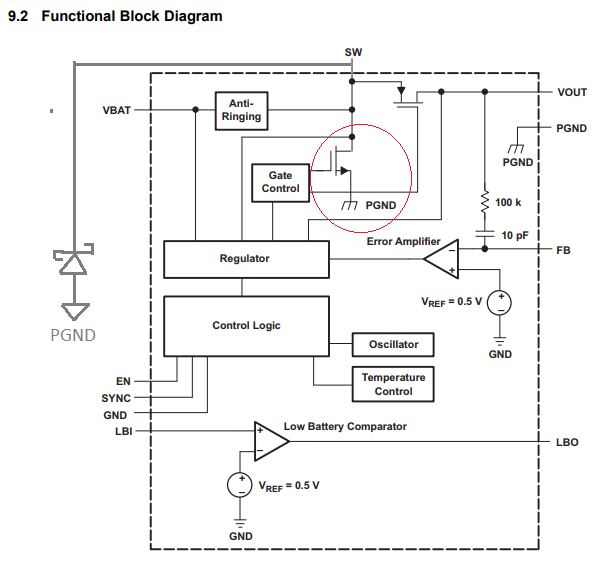
SCHEMATIC:
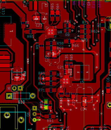
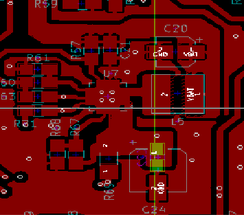
GERBER VIEW:
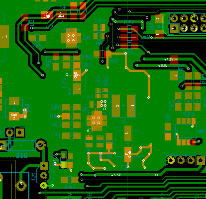
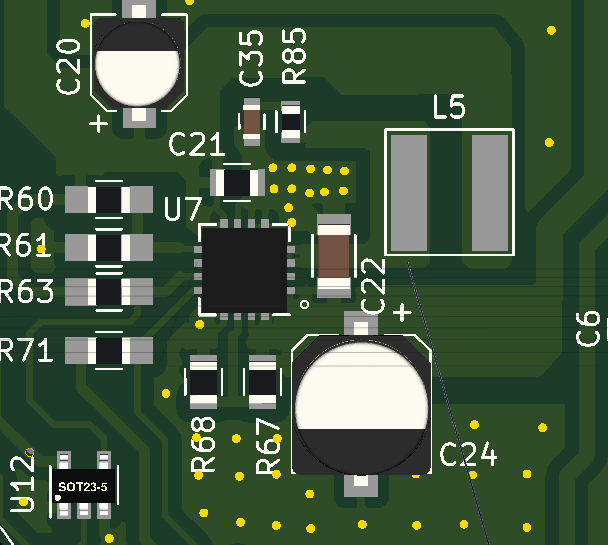
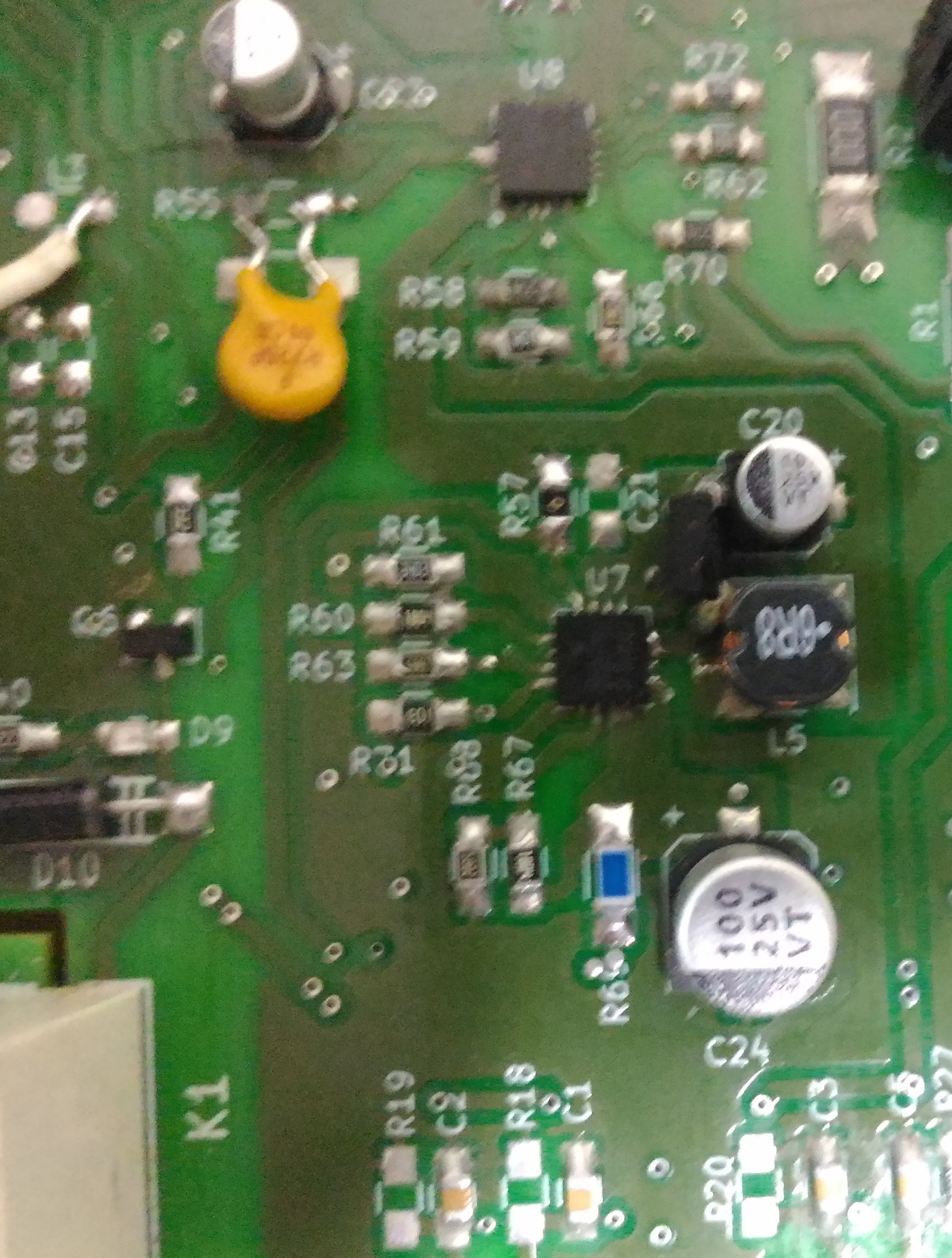
PCB TOP VIEW:
I have gone though some forum articles and found a similar issue on this post
https://e2e.ti.com/support/power_management/non-isolated_dcdc/f/196/t/435455
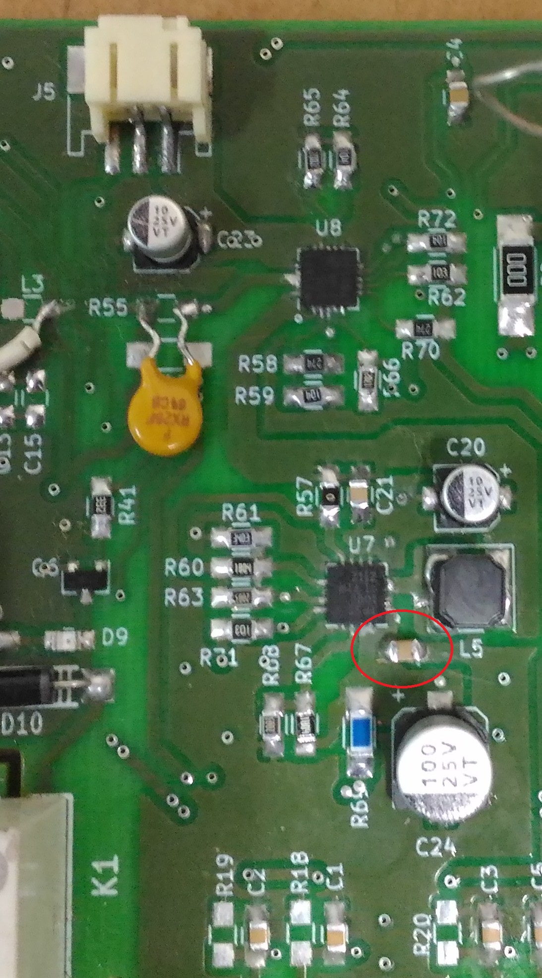
So we tried putting a Schottky diode of 100V rating which we had in stock to see if there was any protection needed for the FET on the gate control. So we kept it as close as to the SW pin. Which can be noticed on above picture of PCB view.
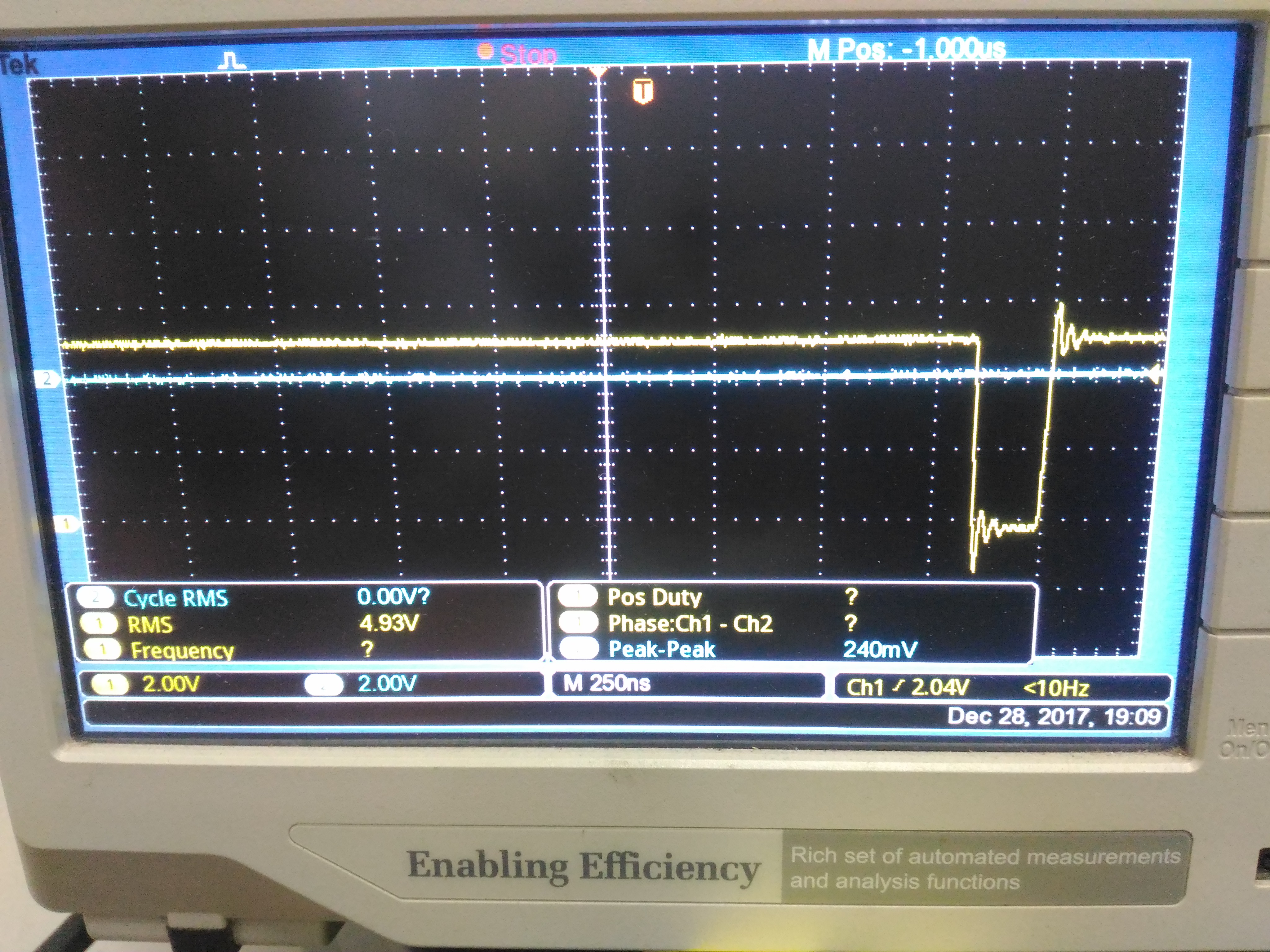
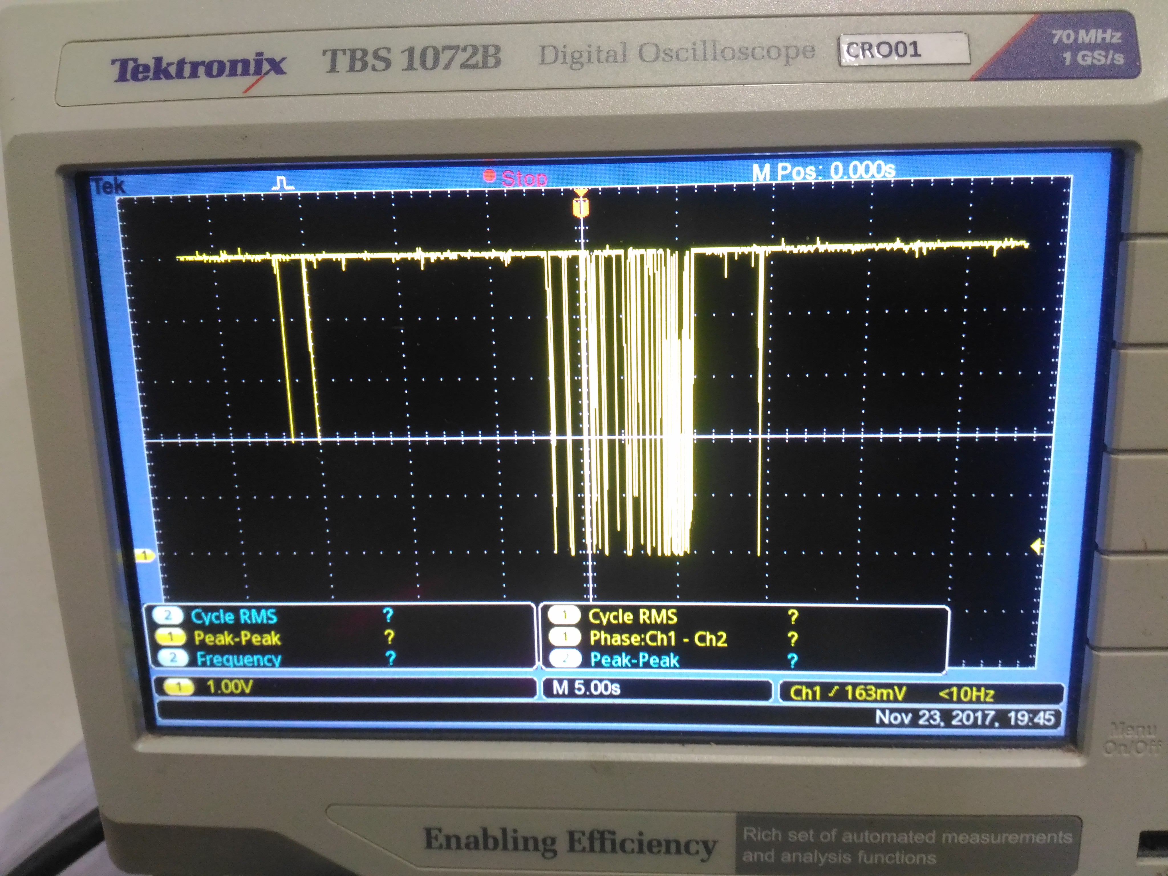
Then after connecting Schottky diode on SW pins 3,4. We turned on the Power supply and got 5V output very stable. But the below some drops in voltages were noticed. We think that these were creating problem and destroying the SW pin. Output voltage totally drops to 0V at some time intervals and some are steady.
The article in previous link also mentioned to use RC snubber circuit across SW pins to PGND which we have not tried yet. The critical 2.2uF capacitor is right below C24 highlighted in Green in Gerber View.
Please also help us selecting the right RC values for snubber circuit.???
Our team will be really appreciated if you help us out sorting this Issue.
Thanking you,
Macjan C. Fernandes
(EME Automation, Goa - India)