This thread has been locked.

If you have a related question, please click the "Ask a related question" button in the top right corner. The newly created question will be automatically linked to this question.

TPS63036: Transition between PWM and power saving modes

Part Number: TPS63036
Other Parts Discussed in Thread: TPS63050

Questions:
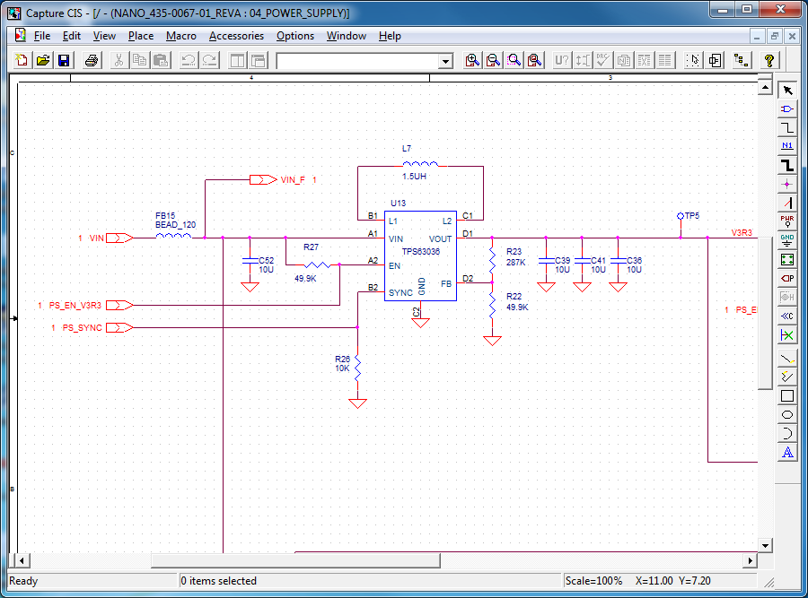
the TPS63036 data sheet, rev October 2015, section 7.4.4 says "If PS/SYNC is set low then power-save mode is entered when the average inductor current gets lower than about 100 mA." and "When the load increases above the minimum forced inductor current of about 100 mA, the device will automatically switch to PWM mode."

From data sheet figure 3, the average inductor current is the average load current plus the (small) resistor divider current. But what is the "minimum forced inductor current"? Also there is no specification on "about 100 mA". What is its range in production devices?

I ask these questions because I have a product in production using the TPS63036. It starts up in low current power saving mode. Great. I then operate the circuit and increase the load current to above 500 mA. For noise concerns I need to be in PWM at that time. Some units are sill in power saving mode. Are the TPS63036's damaged or not? They still regulate, ramping up and down in the power saving mode. Forcing PS/SYN=High does cause PWM mode as expected, but that is a change for my production product. I don't want to ship product with a latent damage. I can't decide if I have damaged TPS63036s without definition of "forced inductor current" and a specified range for "about 100 mA".

Please advise.
Thanks,
John

  • Also there seems to be hysteresis between the power save => PWM transition and the PWM => power save transition. Good for avoiding chatter, but again how much hysteresis should there be by design or specification?
  • Hi John,

    The forced inductor current is the output current in buck operation and input current in boost current. As you notice the transition point between PFM and PWM mode is not specified , about 100 mA is to give an indication, but at 500mA the TPS63036 is expected to be in PWM mode, I am surprised they are in PFM mode.
    "Some units are sill in power saving mode." how do you see this ? Could you share a waveform ?

    Could you precise the operation comditions? (Vin vout and Iout )
    Could you share the schematic and layout?
  • Hello again Sabrina.

    Schematic and layout are same as in our "TPS63036 Start Up" forum exchange, starting 2016/04/25. Copied below for benefit of other forum readers: (Aside: That other exchange resolved with 50 mSec minimum shut down duration.) Back to the current transition from power save to PWM.

    I can see the TPS63036 is in power save mode by the ripple on it's 3.3 volt output, and on the input voltage changes in response to the burst of current when the TPS63036 goes active. Scope capture below, Sope1. I don't currently have access to the TPS63036 switching node.

    Operating condition: 5 volts input nominal, and for these scope traces. Voltage out 3.4 volts nominal, typically 3.36 volts. I have revised my estimate of the load current for the scope traces to 260 mA based on power in. My 500 mA in the first post now seems to high. I don't have easy access to measuring output current. 260 mA is still well above the 100 mA nominal transition point to PWM. (And most other units are in PWM at this load condition.)

    The second scope capture, Scope2, shows TPS63036 operation with PS_SYNC high, 5 mVpp of wander with 3 mVpp,  2 MHz ripple. Looks good.

    Scope 1, PS_SYNC = Low.

    Yellow = Vin, AC coupled, 5 volts DC.

    Purple = V3R3 output, AC coupled, 3.36 volts DC nominal, ~150 mVpp.

    Scope2, PS_SYNC high:

    Yellow = Vin, AC coupled, 5 volts DC.

    Purple = V3R3 output, AC coupled, 3.36 volts DC nominal, ~5 mVpp of wander, 3 mVpp ripple.

    Note the ripple of the Yellow input does not exactly match the ripple of the purple probably because there is an additional switching supply operating in parallel with the TPS63036. Yellow input shows a beat note between those two synchronized power supplies.

    Schematic:

    Layout:

    There is a continuous ground plane one layer down. Via in pad connection to ground.

    https://e2e.ti.com/cfs-file/__key/communityserver-discussions-components-files/196/TPS63036_5F00_Layout_5F00_1.png

    Thanks for your review.

    John

    PS> Please define "PFM", your term for data sheet "power saving mode". Thanks.

  • Scope1

    Scope2

    Schematic

    https://e2e.ti.com/cfs-file/__key/communityserver-discussions-components-files/196/TPS63036_5F00_Schematic_5F00_1.png

    Did this paste??

  • Scope1_scope2_paste thru.docxAnother trry...  This is a might frustrating.

  • It pasted correctly, this time!
    Yes looking at the Vout ripple is one way of telling weather the device is in PFM on PWM.
    I see that the layout has not been modified, the output cap is not placed as close as possible to the device, this may cause higher output ripple.

    By looking at the scope plots, it looks for me expected behavior.
    If the output current is really 260mA the device is usually expected to be in PWM. But looking at Fig 5, 6, 7 and 8 I seems to me there are some operating conditions where the device may still be in PFM mode at 200mA (green curve on Fig 5)

    What is the main concern here?
    - If it is the Vout ripple, in order to mitigate it you can use higher output capacitance (we do no have a upper limit for this device) or use forced PWM mode (would this be an option)?

    - Could you try to apply a resistive or use an electronic load on Vout and detect the entry point PWM mode?

    BTW PFM means "Pulse Frequency modulation" used in Power Save Mode, but you are right in this case it is good to be consistent in the wording even if I meant the same.
  • TPS63036_PWM_vs_Burst.docxI see your note about the jump in the green trace of TPS63036 Data Sheet figure 5. That very much looks like the jump from power save to PWM happens between 200 mA and 250 mA.

    The main main concern is: Are devices that exhibit the transition from power save to PWM at significantly higher than "about 100 mA" defective or have latent damage? It appears not, but I'd like to here a representative from TI say "These devices are not defective." I do wish that TI had put a specification on this parameter, because without a specification how does one decide?

    We are changing our control to set PS/SYNC high to force PWM and remove  the variability of the power save to PWM transition. Ripple when in PWM is fine and only 2 to 5 mVpp in this design.

    I have collected the resistive load data as you suggest. I used the unit I believe has highest transition to PWM. Plot attached (I hope!). Clipping in resistor I'm in PWM until above 250 mA. At 290 mA to 370 mA the unit has a preference for power save mode (because I clip in various resistances always rising current form the open circuit side of the graph). The circuit can be tricked into PWM mode by reducing the input voltage (to increase the input current level), and then returning the input voltage to 5 volts. Average Load currents above 370 mA are required to guarantee PWM mode. From the schematic design values I estimate the inductor ripple current is also about 374 mA, which implies a maximum and minimum forced inductor current of Iave +/- (Iripple/2) = 557mA max, 183 mA min.

    So 183 mA is 80% larger than the "about 100 mA" forced inductor current, the current required  to guarantee PWM with PS/SYNC=low. Normal process variation or damaged component?

    Calculating the max and min forced current, and finding the minimum of 183 mA does feel a lot better than thinking in terms of the 370 mA average.

  • To answer your question: I don't expect the devices do be damaged for such a description, otherwise the device would not work properly in PWM too.

    This device was done 10 year ago, at that time having low output ripple was not the main concern and we have the forced PWM feature to adress this. The PFM/PWM transition point is not a controlled parameter otherwise it would have been in the electrical spec. The newer device have this specified.

    What are the maximum output current required by the application? the TPS63050 may be a could fit