This thread has been locked.

If you have a related question, please click the "Ask a related question" button in the top right corner. The newly created question will be automatically linked to this question.

SM72295: Questions about SM72295 Implementation

Part Number: SM72295
Other Parts Discussed in Thread: TIDA-00120, TIDA-00121,

We followed the PMP7605 reference design in creating our own MPPT controller. (We used an STM32F410 CPU in place of the MSP430 however)

As I have never worked with this type of circuit at this low level, I need to get some additional information about what I am seeing in terms of it's operation before I proceed with connecting a lead acid battery to V_OUT and a solar array (or a current limited power supply) to  V_IN.

As of now, I have only connected a 12v supply to V_OUT in order to power up the board and perform functional testing of the processor and to look at how I am switching the gates of the MOSFETS. One of my observations is that voltage appears at V_IN to GND which is roughly 2x V_OUT i.e.12v at V_OUT gives me 24v at V_IN. Is this normal behavior for this circuit? (I am aware that I will need a blocking diode to prevent the battery from driving the solar array) Aside from any leakage through the upper MOSFETS, should I expect to see voltage at V_IN? If so, what should I expect that voltage to be? Another observation is that when I am not driving the MOSFETS, I have my supply voltage at on V_OUT  appearing at V_IN and am assuming that this is due to the body diodes conduction in the upper MOSFETS.

I would also like to get some clarification on how to drive the MOSFETS in the bridge circuit, Currently, I alternately drive HOA / HOB on, LOA /LOB off and then HOA / HOB off, LOA /LOB on. Is this the correct way to drive the bridge or should I only be switching one side at a time as opposed to both in parallel?

  • Hi Nicholas,

    Thanks for asking about SM72295. It seems you are wiring your interleaved buck in reverse as an interleaved boost.

    The proper way to switch an interleaved buck or 2-phase converter is to interleave the main switch or highside 360deg/n-phases=180deg out of phase similar to the lowside, similar to Figure 1 in the link:
    www.ti.com/.../slva882.pdf
    PMP7605 is the test report of TIDA-00120 which switch node waveforms can be found here on page8:
    www.ti.com/.../tidu219.pdf
    more info on interleaved buck here:
    www.ti.com/.../slyt139.pdf

    The questions of a buck converter still apply, If 12V is applied to the output and the input has a voltage double the input, that may mean that you are running the converter backwards since the flow of power in buck is proportional to duty cycle. Which by the definition D=Vout/Vin when Vout=12 and the converter is set to regulate the output to 12V and Vin=24V then D=50%. Can you confirm the dutycycle? If 50% then this is normal behavior for a buck converter ran in reverse.

    If both LO are applied simultaneously when 12V is on VOUT then both inductors will charge since the lowside is now the main switch (like a boost converter). After charging the inductor and shutting off LO the stored current follows the path of the HO body diode and after HO is turned on, current is allowed to flow in both directions because it’s a synchronous and therefore reaches VIN.

    From the boost converter point of view (with 12V on VOUT) the PWM control technique has nothing to do with it, that is with interleaved switching instead of simultaneously switching the converter applies pulses to the main switch, LO regardless and therefore applies some charge to the inductor. HO does not have to turn on because the body diode will conduct when the inductor current stops flowing through Lowside switch and continues to VIN through the highside. With the interleaved method and 12V on VOUT the converter will achieve regulation manifesting 24V on VIN.

    Please let me know if you have any more questions!
    Thanks,
  • Thanks Jeff!

    >> It seems you are wiring your interleaved buck in reverse as an interleaved boost.<<

    I suppose this is the case since I am applying a source to the output i.e. where the battery to be charged will be connected. It is easy to see why the circuit works in boost mode from Vout to Vin (or in buck mode for that matter). I can confirm that I am currently operating at a 50% duty cycle so the boost voltage I am seeing is correct.

    From your explanation and from Figure 1 of slva882.pdf, it looks as if I should be driving the Phase 1 MOSFET gates of HO and LO 180 deg out of phase and then the gates of phase 2. In other words, (looking at it from the buck direction) for phase 1, I would switch on HO, connecting Vin to Vout and allowing the inductor to charge through that circuit. I would then switch off HO and switch on LO after a dead time, which would allow the inductor to discharge through Vout. I would then then repeat this sequence for phase 2. Is this essentially correct?

    Also, it seems that I am wrong in switching my 2 phases in parallel i.e. HOA / HOB on and then LOA / LOB. It seems that I should only have 1 phase active at a time i.e. HOA (dead time) LOA (dead time) HOB (dead time) LOB (dead time).

    It looks as if slyt139.pdf has some additional information on switching frequency that I will want to review. For now, I was planning on running the converter at around 200 kHz as in the eval board. I looking for some additional insight into optimizing the dead time between driving the HO and LO gates.

    So, it seems that I should be seeing some level of boosted voltage at Vin i.e. at the point where we connect a solar panel. I was planning on using a current limited power supply in place of a solar panel for testing but am rather leery about doing so since the voltage at this point gets rather "high" (if you can call 24v a high voltage) but certainly high enough to damage the supply if I don't do something like implement a blocking diode. It certainly seems that when I charge a battery to, say, 13 volts, I could likely see 26 volts across the solar array or Vin power supply, dependent on duty cycle.
  • Also, I am wondering if I can get you to review our schematic and layout to verify that everything is correct from your POV?
  • Hi Nicholas,

    Thanks for the update, feel free to send any schematic I would be happy to review with you. I should have mentioned this app note:

    http://www.ti.com/lit/an/slyt449/slyt449.pdf

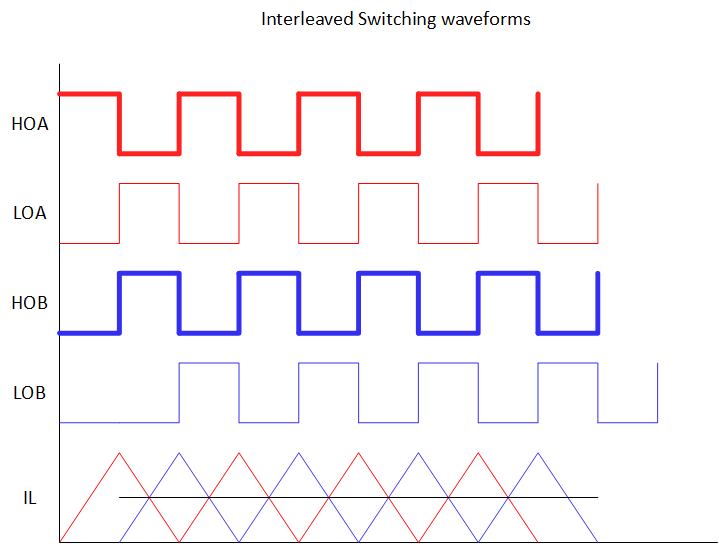
    The interleaved part of the buck triggers HO at 180deg opposed to triggering both HO’s at the same time at 0deg like you are doing now. Each half bridge leg should of course be operated complementary as to not prevent shoot through. I made this diagram to help making this explanation clear:

    Interleaving reduces ripple and in turn RMS current. It also doubles the filter frequency so smaller components can be used. By triggering HO alternately hotspots can be reduced and since the duty cycle is 50% this app note explains it will give you max ripple cancellation since one phases current peak occurs when the other phases trough occurs. This ripple reduction ultimately increases efficiency since more current is being consumed by the load as average current.

    For deadtime optimization. Assuming you want to optimize it for CCM and want time smallest time possible. For steady state conditions DT is constant however it needs to be varied during a load transient for example. A recent app note on deadtime optimization is for high speed GaN drivers but still applicable to FETs and what to look for in a half bridge configuration: http://www.ti.com/lit/an/snva815/snva815.pdf - page 4 - minimizing dead time

    SM72295 has 1ns of delay matching from input to output between the two HO/LO channels. There are TIDA’s using SM72295 that implement 80ns deadtime with no problem, how small of a DT are you needing? For DT’s as low as 4ns there is a TI driver control method called adaptive deadtime control however not used on SM72295.

    For the current limited supply in place of the panal on VIN, are you using the normal blocking diode from the solar panal to the battery (so the battery cant dischange into the supply)? are you worried about the VIN-panal voltage going above 26V and damaging your 25V supply?

    Thanks,

  • Thanks Jeff, the new appnote and your timing diagram really helps to clarify things.

    I attached a .zip of the schematic and another one that contains the layout gerbers.

    >>how small of a DT are you needing?<<

    I don't really have a specific dead time in mind; as I understand it, we lose efficiency with greater dead times so I would want to use the least amount of time that would prevent shoot through. The STM32F4 allows me to program dead time between the complementary channel outputs I am using to drive HO and LO on each phase. If the SM72295 has 1 nS of delay time between HO and LO, I may be able to program my dead time to 0 but the last time I tried this, I wound up drawing excessive current from my power supply (connected to Vout) OTOH, I was not driving my phases as you recommended above so I may want to try experimenting with programming the dead time again

    >>For the current limited supply in place of the panal on VIN, are you using the normal blocking diode from the solar panal to the battery (so the battery cant dischange into the supply)? are you worried about the VIN-panal voltage going above 26V and damaging your 25V supply?<<

    I did not have a blocking diode in place but I do now. It looks like this circuit requires it. The charge controller design we currently rely upon (it's a linear design as opposed to a switching design) employes an additional  MOSFET in line with the charge path that remains off until the solar array voltage > battery voltage so we did not require an extra blocking diode. 

    Under normal operating conditions for this circuit, say with a battery charged to 12v connected, what is a "typical" range of voltages I may expect see at the solar array, assuming that I vary the duty cycle between 30 % and 70%? Does the equation DC = Vout / Vin apply? Do you have any recommendations for blocking diodes? 

    781-020-003-revA.zip

  • Hi Jeff:

    A couple of more questions

    Looking at the schematic, you will notice that I have the ability to disable the VCC supply (12v) to the SM72295.

    Do I risk damaging this part, or the processor,  if I continue to drive the LI and HI input pins from the processor timer outputs with VCC disabled? (but having VDD (3.3v) still enabled)

    Also, what kind of operating current (not including charge current)  can I expect to draw from the battery connected to V_OUT (J2) while switching the phases? I am seeing about 100 mA. We need to reduce this as much as possible since we are powering everything from the battery connected to J2 and this charger will be constantly connected to the battery, drawing some amount of quiescent current, even during shipment. Disabling VCC to the 72295 gets me down to about 15 mA. but I want t verify with you that I can safely power down this part without causing other problems.

    Another question, related to one I posted above: Given what I know so far about the relationship of duty cycle to Vin and Vout, it looks like I can realize voltages of up to 50 volts at Vin under certain conditions, say if we connect a battery charged to 15v to Vin while switching at a 30% duty cycle. Does this seem right? 

  • Hi Nicholas,

    Sorry for the late reply, I will update you on the schematic review in 24 hrs.
    Thanks for letting me know all this info. All this is great for e2e threads and the more we have the better.

    The switching solar charge controllers use MPPT to track the panel voltage and squeeze as much current out before the output drops. The voltages on VIN should follow the same buck equation as long as your switching waveforms are the same. With a 30% dc and VOUT=15V then VIN is expected to be equal to 50V. The VIN input current should be a function of the output current. So if you are seeing 100mA at VOUT then you should be seeing 30mA for VIN because IOUT = IIN/D while neglecting power losses.

    Both TIDA-00120 and TIDA-00121 have FETs for blocking diodes like you mentioned. TIDA-00121 is also similar solar charger. Is Q6/Q15 in your schematic normally ON in which the FET’s body diodes would be acting as the blocking diode? I will take a closer look at your schematic and update you asap.

    Its possible to fine tune the driver output delay from gate on/off resistors or Cgs capacitors to accomplish 0ns dead time from the MCU to get an optimal efficiency but its safer to have some deadtime. Besides dead time loss, the smaller the power stage FET’s Qg the better the efficiency since for higher-frequency switching-losses prevail which are proportional to Vdd^2*Fsw*Cg.

    Thanks for coming me to verify risk. There are no known cases of damage from an input PWM if VDD is present but VCC is not or vice versa for SM72295. As an action, I will grab a SM72295EVM and run a non-char bench test to confirm that the inputs can withstand power cycling VCC while 3.3V 200kHz and VDD=3.3V. My guess is there is no problem at all and that the both UVLO’s go into effect since VCC is less than the UVLO threshold of about 6V. During UVLO both outputs are held low and HB-HS UVLO with only hold the highside low.

    Thanks,
  • Hi Jeff:

    Concerning dead time: I am able to program the dead time between the complementary timer outputs that drive the gates of each MOSFET pair. I am finding that I need to introduce a minimum of 5 uS of dead time between these signals to avoid shoot through when operating between a 30 and 70% DC at a switching frequency of 200 kHz. This seems excessive to me. If I reduce the switching frequency to 100 kHz, I find that I cannot deviate too far from a 50% DC even when substantially increasing the dead time without encountering shoot through.

    I am wondering if the CSD18502 MOSFETS we used in the design are too slow?

    Another question about switching.... Since I am driving the low side MOSFETS with timer outputs that are complementary to the high side MOSFETS, (i.e. I'm using 1 timer on my processor that has 4 outputs, 2 outputs drive the hi mosfets and 2 complementary outputs drive the lo mosfets.)... the duty cycles between the outputs are also complementary, that is, when I'm switch the upper MOSFETS @ 70%, I am switching the lowers at 30%. Is this acceptable?

    One more question: Given the above, I observe that I cannot realize voltages at the solar array connector (V_IN) that are lower than about 22 volts.  As I understand it, I should be able to adjust the voltage across the solar array within some range around the optimum operating voltage of the array... about 17 volts. With the circuit as it is, it seems that we will never be able to charge a battery from the solar panel.   

  •  

    Hi Nicholas,

    Thanks for the update and great questions and understanding, and that’s a lot of deadtime! I would like to have a look at all 4 input signals, it seems that the half bridge is not being switched correctly. If everything is switching correctly, referring to my handy dandy 'interleaved switching waveform’ red/blue diagram you should have 2 timers driving HOA & LOB likewise you should have 2 complementary timers driving HOB&LOA, can you confirm this?

    Check this article out on interleaved bucks but our buddy here at TI - Marcus Zimnik -

    I attached my first pass on your schematic, there are a few Q/As maybe we can tackle. I will take a second pass with fresh eyes and update you with the SM72295EVM PWM-powercycle test results by monday.

    Thanks,

    mppt-ems_sm72295 jeff edit1.pdf

  •   Hi Jeff:

    I cant access the questions on the schematic. Perhaps you can post them in another way.

    Your timing diagram was very helpful. Hopefully, TI will include it in a future rev of the 72295 datasheet

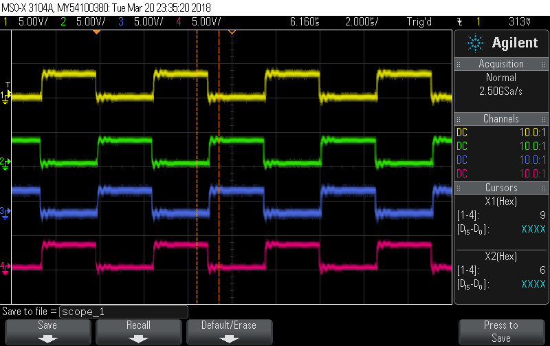
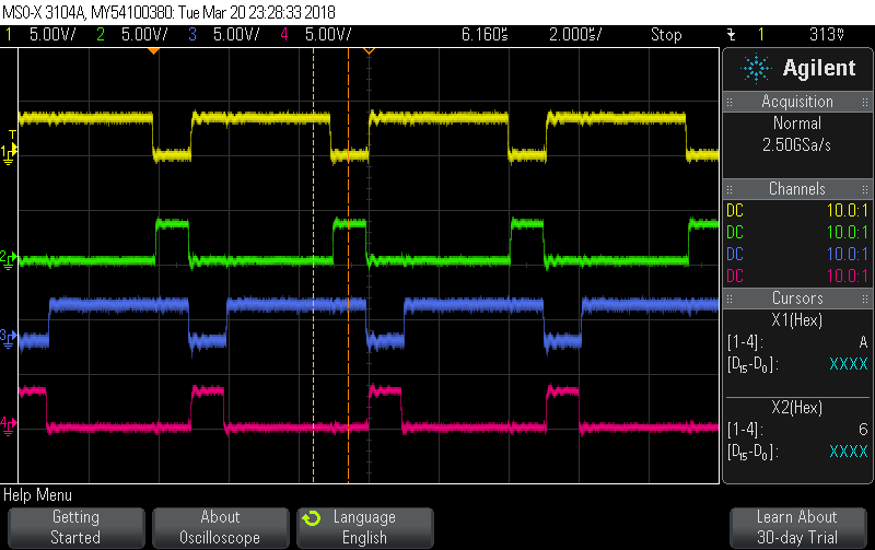
    I attached scope shots of the LI and HI signals I now have. Going from top to bottom... HIA, LIA, HIB, LIB.

    The top shot is a 50% duty cycle, the bottom is 80%.

    The ringing in the traces is due to less-than-ideal scope probe grounding,