This thread has been locked.

If you have a related question, please click the "Ask a related question" button in the top right corner. The newly created question will be automatically linked to this question.

LM5170EVM-BIDIR: Special 12v Application (Buck Mode Only)

Part Number: LM5170EVM-BIDIR
Other Parts Discussed in Thread: LM5118, LM5170, LM5170-Q1

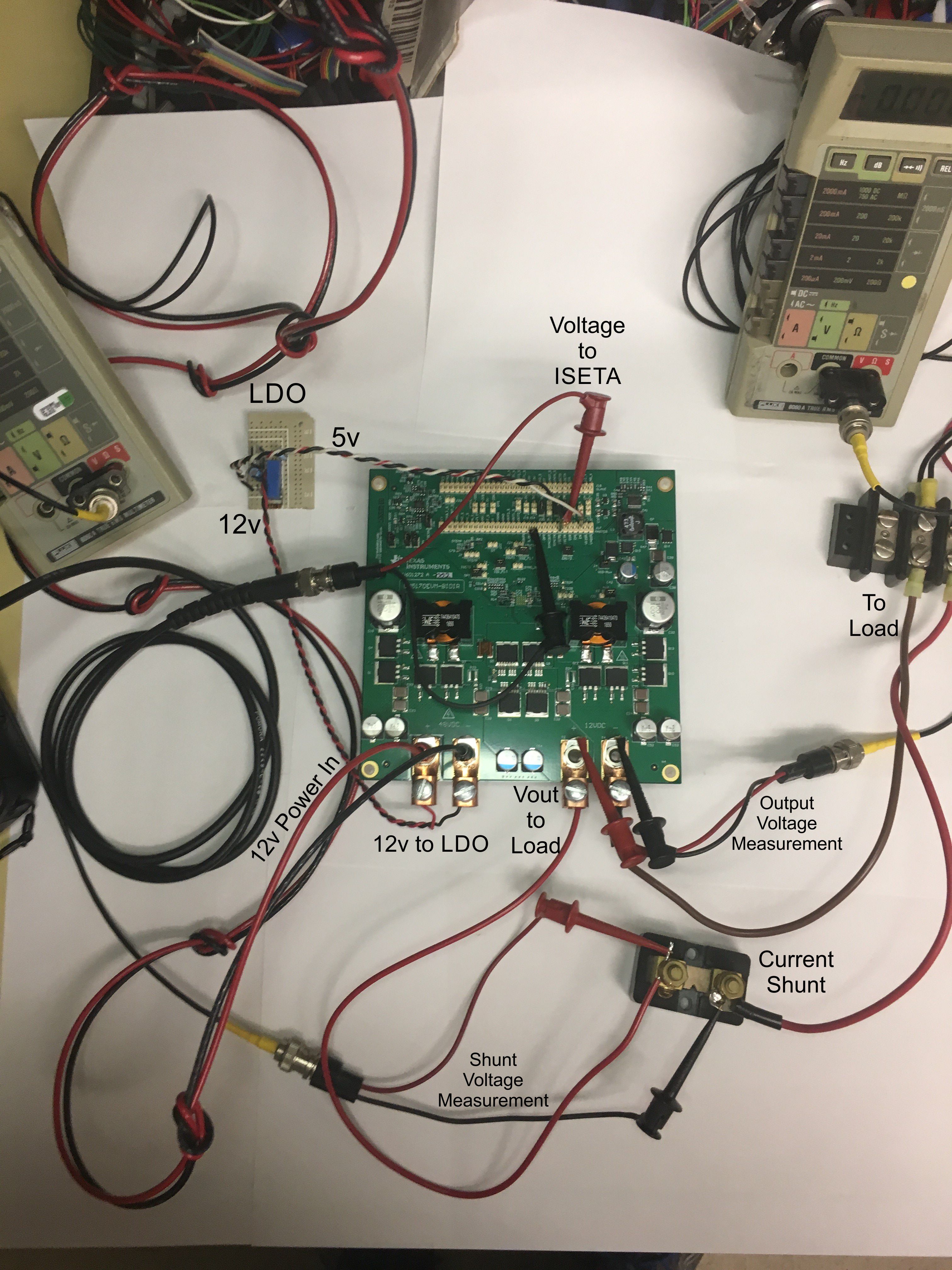
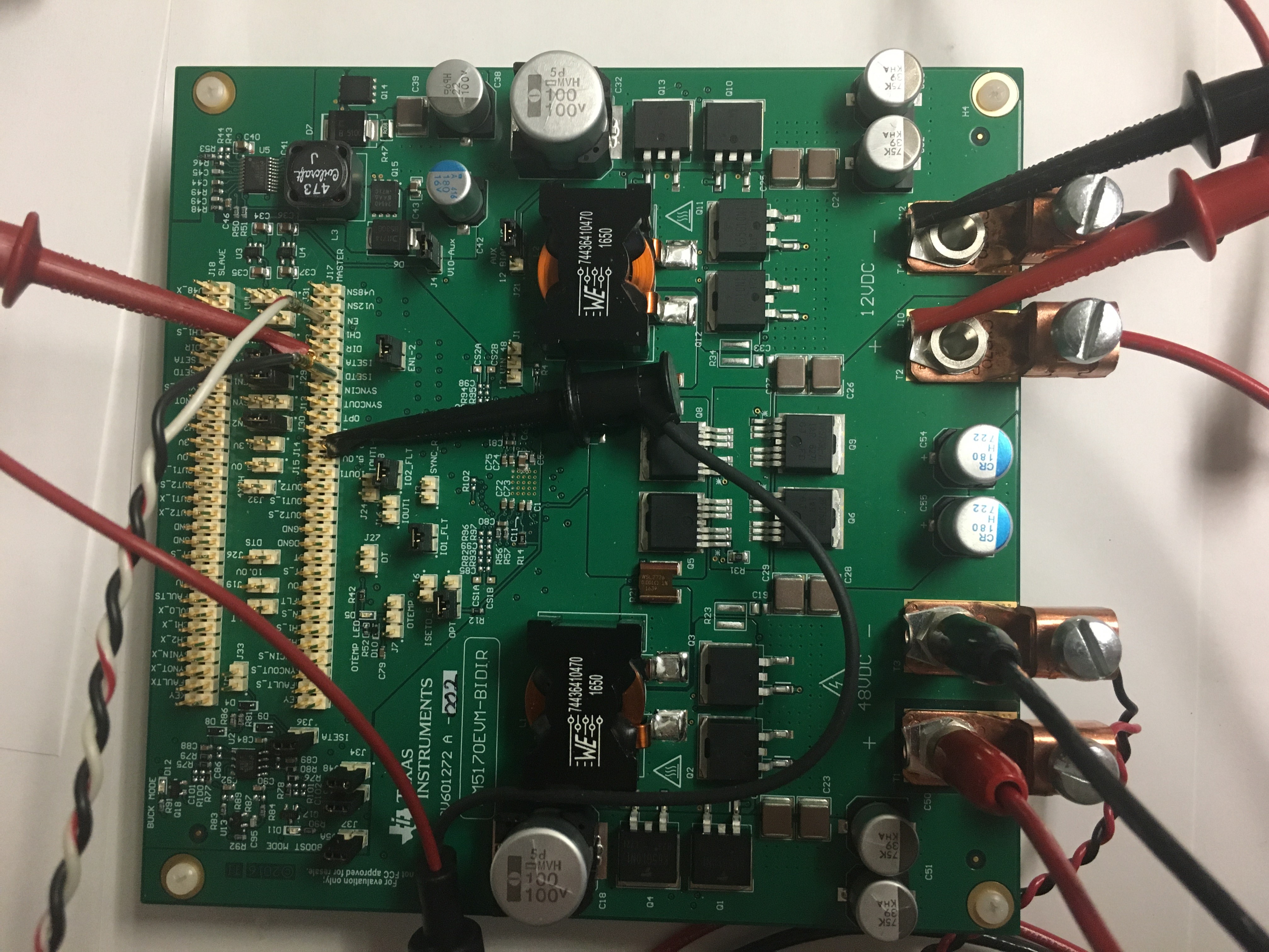
I have a low volume (test apparatus) project that the LM5170EVM-BIDIR will fit perfectly if I can configure it to do the following:

1) Self-start upon the application of primary (input) power.

2) Input voltage could range from 10v to 16v

3) Operate in the "Buck Mode" only

4) Allow the output voltage level to be controlled via an analog signal source (potentiometer or other voltage source)

5) The output voltage would be varied, set, and regulated and could vary from 95% to 60% of the input voltage (Again, Buck Mode Only)

6) Operate in the 2 phase mode with the option of the stacking to a 4 phase mode depending upon the power level needed for the application

7) ...

I have developed, designed, and fabricated this type of apparatus using another manufacturer's Buck/Boost converter EVM and found that unit to be far more complicated than is desirable. Especially regarding what mist be done for the startup sequence upon power up. I'm hopeful that the LM5170EVM-BIDIR will be much simpler in this regard and the scalability  of this converter (through stacking) will offer some serious benefits also.

Many thanks for your time and consideration!

Dan Hagan

  • All these can be done easily. You do need to produce the 10V bias voltage to feed VCC, and this can be done with a simple regulator. The EVM used the LM5118 but it was intended to supply 10W for multi-board-multi phase integration. You only need one VCC bias supply for multi LM5170 running in paralleling.

    The EVM was designed to support many different configurations which may appear excessive for any given application. Simply removing those unused features, jumpers and circuits, then you can get a much clean circuit.

    Start from the EVM schematic, and you can cross out the circuits not used for your application. Good luck.
  • Youhao,

    Many thanks for your kind reply and advice...

    I have my EVM strapped (J4 is closed) to use the internal 10v supply for Vcc. What is not clear from the documentation is whether or not the onboard Vcc supply will be energized as soon as a voltage is applied to the input (48v) terminals (T1 & T3). This mode of operation makes perfect sense; but I don't like to assume anything.

    All the 3-pin headers are set at the defaults:

    [Sorry, I guess images aren't allowed...]

    Most of the 2-pin settings are set at their default with exceptions as noted X:

    What the image depicted was that all the 2-pin settings were at default except for J4 (onboard Vcc) and J25 (dual channel enabled).

    Another problem that I've run into is that the EVM schematics that are offered via a link referenced (on page 22) in the document "snvu543a.pdf" [LM5170-Q1 EVM User Guide] doesn't work.

    Also, does the EVM require a load on the output terminals (T2 & T4) to function and if so what minimum a load would be needed?

    Many thanks!

    Dan Hagan

  • SV601272A(002)_Sch.PDFFirst, the schematic is attached.

    It does not require a min load.  The output terminal can be open, and the original EVM with the voltage loop closed,  namely J34, J35, J36, and J37 jumpers closed, you should get the output at about 14.5V.

    Note that, to use the onboard bias supply, you need to close J21-Pin2-3 (the right side labeled 48) when your source is on the 48V-port. You also need to separately pull up the the UVLO pin (J17-Pin5, labeled EN, but not the one next to the label, but the other pin on the same column) to >2.4V, to start the operation.  Pin 6 and other pins on the same row of J17 are GND pins. This is the master enable and must need an external pull up on this EVM.

    Hope these help.

  • Youhao,

    Many thanks for your suggestions as I now have a working "buck" converter EVM and am able to control the output current via the ISETA pin J17-11. I have two more questions:

    1) I currently have a resistive load on the unit that draws 8 Amps @ 7.5v output (T2 & T4) with 12.1v at the Input pins (T1 & T3). I believe that I have the EVM strapped to run in 2 phase mode as I have J29 & J30 Closed. At this power level the EVM MOSFETS Q5, Q6, Q8, Q9 become quite warm after about 3 minutes and I wouldn't expect this to happen considering the high efficiency levels at which these converters operate. Am I doing something wrong? What do you suggest I check???

    2) My application requires a regulated (set) voltage output. I can vary the output current (with a fixed load) and it works very well as I can control the current level via ISETA (J17-11) from 0 Amps to a maximum of about 8 Amps @ ~7.5v for the fixed load that I have on the EVM. Is there a configuration for the EVM that allows for a regulated voltage output? If the answer is in my documentation I apologize for bothering you...

    Again, many thanks!

    Dan Hagan
  • First, the output voltage can be regulation with the outer voltage loop built in the EVM. The circuit is on the upper left corner and you need to close jumpers J34-J37 to enable the voltage regulation. Changing the resistor dividers you can set to different output voltage setting.

    At 8A the MOSFETs should not be warm. I am afraid these FETs are not fully turned on, and somehow got damaged. If you done need them, you can remove them and short a copper foil on the back side across the two exposed copper pad beside D3.
  • Youhao,

    Regarding voltage adjustment (control)

    J34-J37 have all been closed since the unit started working in the buck mode. What I didn't realize was that by varying the ISETA voltage level between 0v and ~1.0v I was able to vary the voltage across my resistive load by (of course) varying the current. After your feedback and further thought I have realized that setting the ISETA to maximum would give me a fixed output level (high current limit) and then the regulated voltage output (setting) could then be done via the resistor dividers you mentioned in your reply. Is there any documentation (guidance) available to suggest values for the divider resistors to achieve the desired output voltage range?


    I agree that the MOSFETS should not be warming up and this leads me to believe that I still have a configuration issue. My understanding is that MOSFETS Q5, Q6, Q8, Q9 are the circuit breaker devices and considering the low power/current that I'm controlling they shouldn't even be active. It might be useful if I could send an image (picture) of my setup with labels to you so that you could see precisely what I'm doing. Is there a way to do this?


    Your patience with me is greatly appreciated! I hope that this long interaction (back and forth conversation) on the forum is not a problem for you or your management.


    Dan Hagan

  • Youhao,

    Here is some more information in image form showing you how I have the EVM connected to the power source, the load, and of course the control voltages.

    And here is a close-up of the EVM so that you can check how the straps are set.

    These are high resolution images that I assume you can download and zoom in on to check any detail that you might need to see.

    Many thanks again for your time and trouble...

    Dan Hagan

  • I see the issue now: you input is only 12V, which is not high enough to turn on the circuit breaker FETs (Q5,Q6,Q8,Q9). You must remove these four FETs and solder a piece of copper foil or thick wire to short the two exposed pad on the back side (beside D1).

    Please read the datasheet page 29 carefully about the circuit breaker feature. And it is also explicitly indicated that "If the steady-state differential voltage between the HV-Port and LV-Port is less than 10 V during power up, TI does not recommend the user to activate the failure detection function. Also, if the differential voltage is less than 8 V, TI recommends not to use the circuit breaker function of the LM5170-Q1 at all."

    Thanks,
    Youhao
  • Youhao,

    I suspected something like this might be the case! Thank you so much!!! I will consider doing as you suggested and remove the FETs and also review the datasheet section you referenced!

    This is very helpful indeed!!! Thanks!

    -----

    I have just now reviewed sections 7.3.16.1 and 7.3.16.2 on pages 28 and 29 of the LM5170-Q1 datasheet. Please consider that at startup the HV-Port is raised to ~12.5v and the LV-Port is at 0v with a resistive load attached. This is more than the 10v minimum specified but perhaps it is too close to the minimum level for the circuit breaker array to function properly. I will be happy to physically disable (remove) the FETs as you suggested but I must first ask if we were to "disable" the failure detection function, would the effect be the same as the removal of the FETs? Here's the text I'm seeing in the datasheet and is the reason I'm that asking the question:

    From section 7.3.16.1:

    To disable the failure detection function, place a 10-kΩ resistor between the SYNCOUT and AGND pins, as shown in Figure 35, and the LM5170-Q1 skips the 2- to 3-ms interval of MOSFET failure detection. Instead, it will activate the standby mode in approximately 300 μs after VCC is above 8.5 V and UVLO is greater than 2.5 V. If the circuit breaker is not present or not controlled by the LM5170-Q1, do not leave the BRKG and BRKS pins floating, but terminate the BRKG and BRKS pins with 20-kΩ resistors as shown in Figure 35.

    Please know that I'm not trying to second guess you on this, but it appears that the 10v minimum issue might also go away if the failure detection function was disabled. If I'm wrong please know that I will be happy to modify all my EVMs as you have directed. Which brings up the following question:

    I expect to be operating at least two EVMs in parallel (4 phase mode) but it is possible that more  power may be needed. Obviously, if removal of the FETs is necessary, all the EVMs will be modified as you have suggested. Will there be any significant risk at the high current levels I anticipate running at -- by not having an "active failure detection function"? Is there some risk to my equipment? Of course there will be external current limiting devices in the overall system (external to the EVMs).

    On another subject...

    I still need your help with-respect-to the voltage setting and regulation using the Outer Voltage Loop Control Circuit. Are there some guidelines for resistor values that would allow the adjustment and regulation of the output voltage independently of current flow? Every component on the EVM is of the surface mount type and I want to be sure which components are to be altered, removed, and substituted to accomplish the function that I need. I will continue to scan the datasheet for the information I need.

    Again, your time and trouble is greatly appreciated!

    Dan...

  • Hi Dan,
    If you disable the fault detection, you can turn the circuit on without removing the breaker FETs. However, what will be your output voltage? The breaker FET driver voltage is basically the differential voltage between the input and output voltage. To be accurate, it is the voltage between the 48V-port and 12V-port of the EVM. If the differential voltage is low, you may not be able to fully turn-on the breaker FET. This is why I think you should remove them to avoid further trouble in your test.

    Thank you for using the part, and wish you good luck.