This thread has been locked.

If you have a related question, please click the "Ask a related question" button in the top right corner. The newly created question will be automatically linked to this question.

CSD95372BQ5M: CSD95372 and CSD95377Q4M / Waveform over the ABS-max

Guru 11170 points
Part Number: CSD95372BQ5M
Other Parts Discussed in Thread: CSD95377Q4M, TPS53661

Hello E2E,

Our customer is using the CSD95372BQ5M and CSD95377Q4M for now board.
They are evaluating it now.

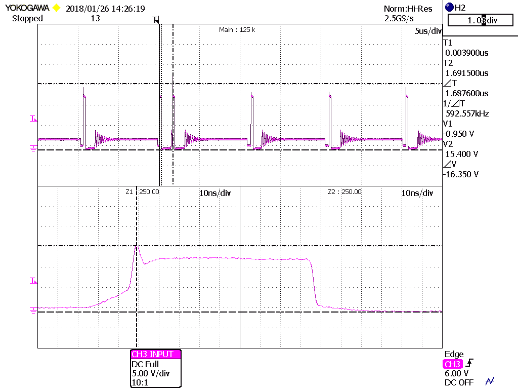
SW-port voltage is over the absolut maximum range.
Please see the attached file.

SW-port voltage of CSD95372BQ5M down to -0.95-V at ON.
SW-port voltage of CSD95377Q4M down to -0.7-V at dead time.

Conditions;
  Contlorler is TPS53661.
  They referred CSD95377Q4M datasheet to layout design for both.

Questions;
  Does TI verified the parasitic inductance for this layout?
   -> Please provide this verified data.
  Can these devices accept the current situation?
   -> If can't there, please let me know the correctry layout.

Regards,
ACGUY

Waveform.pdf

  • ACGUY,
    Thanks for posting. Let me consult some experts on these parts and the recommended layouts on their datasheets to see what they think. Hopefully I will be able to get back to you within 24 hours.
  • Hi Brertt,

    Thank you for reply.
    I expect for your comment coming.

    Best regards!
    ACGUY
  • ACGUY,

    I spoke to our experts. We really can't provide a useful number for the parasitic inductance of the layout, because this is a strong function of the board stackup and the PCB thickness. 

    However, the waveforms you are showing are fine and what we would expect for this application. The switch node and PGND normally goes from ~-0.7V to -1V while the body diode is conducting. The -0.3V spec in the datasheet is meant to be a DC spec only. Body diode conduction during switching events is normal and will not hurt the part. 

    Hopefully this answered your question but feel free to let me know if you have any more questions. Thanks!