Because of the holidays, TI E2E™ design support forum responses will be delayed from Dec. 25 through Jan. 2. Thank you for your patience.

This thread has been locked.

If you have a related question, please click the "Ask a related question" button in the top right corner. The newly created question will be automatically linked to this question.

UCC28711: UCC28711 operation

Part Number: UCC28711

Hello,

I have designed a 120W flyback by referring to the design document of tidu412a.

Link: http://www.ti.com/lit/ug/tidu412a/tidu412a.pdf

My design specifications are :

Input:300V to 900V

Output: 24V, upto 5A

Transformer number of turns: Primary/secondary/auxiliary 176/16/11

Airgap: 3mm

With the current design, I am getting the output of only 1.76V at no load with an input of 350V.

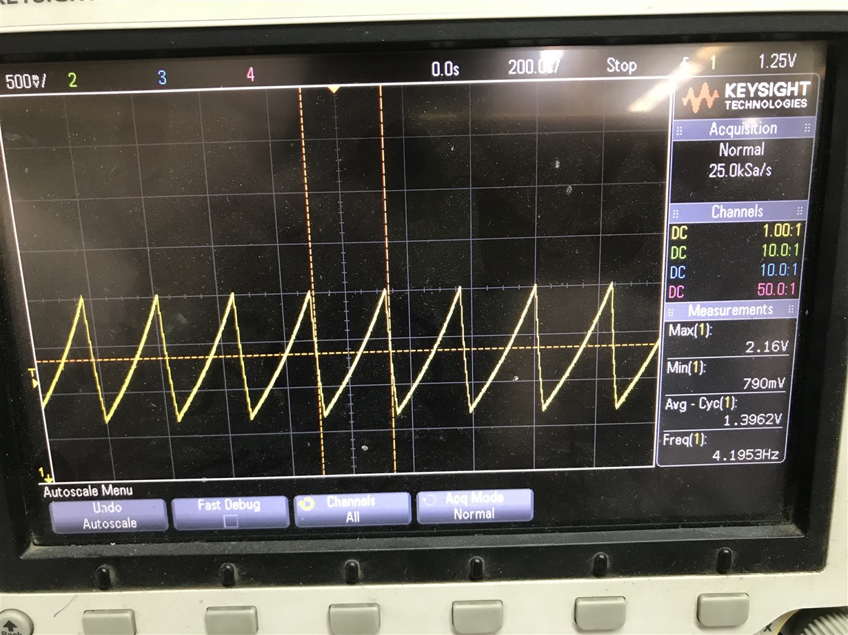
I am not able to understand what is wrong. My IC is not giving output PWM at DRV pin. The voltage at VDD pin is going above 21V and suddenly decreasing to 8V

and this continues, means, my IC is not starting. I tried replacing the IC, that didn't help. Please suggest what next to do. The schematic file is attached.

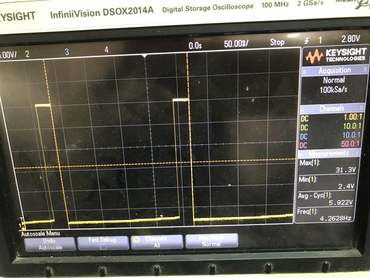
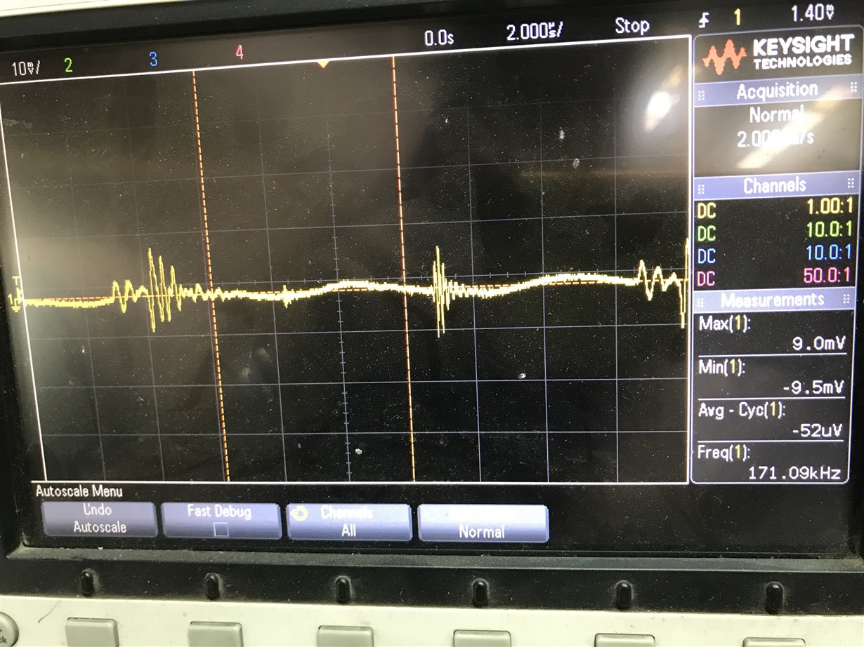
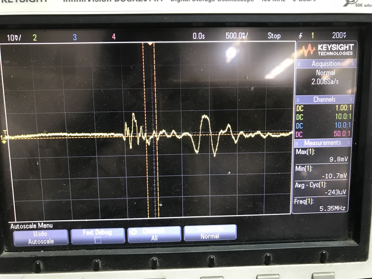
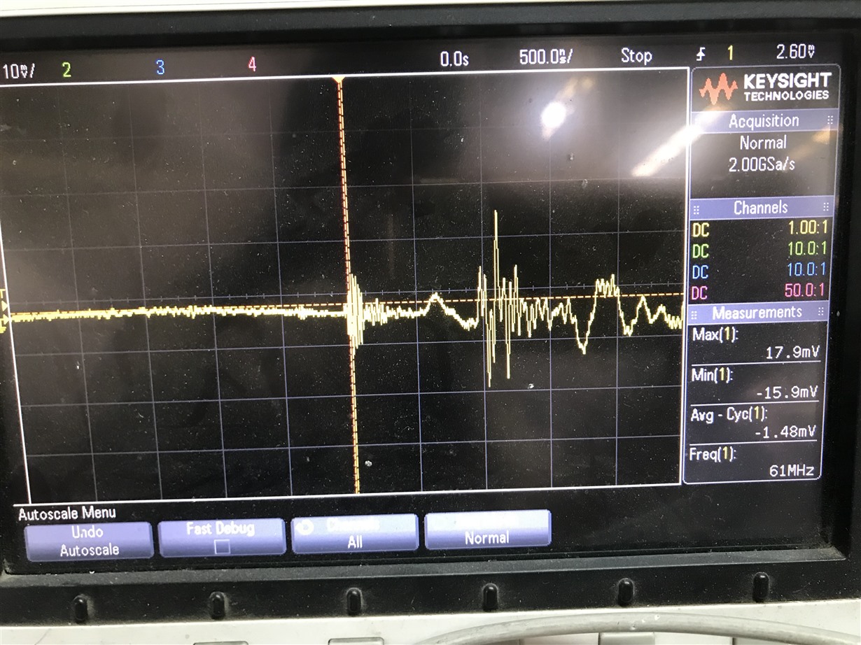
The related waveforms are given below. (The probe has a multiplier of 10, means please multiply 10 the voltage values shown in the waveform images)

HV pin waveform:

CS Pin Waveform:

VDD Pin waveform:

VS Pin Waveform

DRV Pin:

Please help me out .....

Flyback v1.0.pdf

  • Hello Punyashree,

    Thank you for your interest in the UCC28711. In the circuit schematic that you provided, I noticed immediately that there is a 120uF cap across the auxiliary winding. Then comparing to the TIDU412a schematic (page 31 of that file), I see that there should be another diode (28) between the 120uF cap and the aux winding. Your schematic is missing that diode.

    As a consequence, each time the VDD voltage reaches 21 V and the controller attempts to start switching, the primary drain voltage reflected to the aux winding applies a negative voltage across the 120uF and this causes a large current spike at the CS input and shuts down operation.

    Please add the missing diode to your design, and things should work better. Assuming that that is the only error, I did not make a further review of your design. But I recommend that you thoroughly compare your schematic to the TIDU schematic and ensure that the rest of the circuit components and their connections are correct.

    Regards,
    Ulrich

  • Hello Ulrich,

    Thank you so much for your reply & support. Adding diode before 120uF cap helped a little, but not much. The frequency of HV pin decreased to 1.7Hz from 4.26Hz. But I am not getting PWM at DRV pin (only 1 pulse, that's all). It was suggested in the datasheet that not to add cap across CS pin. So previously I didn't use any cap. But for testing, as highlighted in TIDU412a  application note, I did experiment adding 330uF cap across CS pin before Rlc but it didn't help much.

    If you have any other idea or solution which I should try, then please let me know. I am kind of stuck in the middle. Please reply back. 

  • Hello Punyashree,

    I'm sorry that you are still having trouble. Apparently there are other issues than just the missing diode.
    One thing I forgot to mention is that VS sensing network R10 + R11 should be connected across the transformer Aux winding ahead of the new diode's anode, not at the cathode across C9. If you've checked your design against the TIDU412a reference schematic, this will not have been a problem.

    Assuming the correct connection, you should be seeing 3 short pluses at the Q1 drain, not just a single pulse. See TIDU412a, page 14, Figure 11. This should happen as long as the input voltage is lower than the programmed start-up voltage.
    Based on your schematic values, R10 and R11 are correct for 24V regulation and ~28V OVP. However, for the given turns ratios, R10 is sized for start-up at ~425Vdc on the bulk voltage rail. If you are testing at 350Vdc on the bulk rail, then the controller should be attempting to start-up with 3 test pulses and then shut down and cycle through UVLO and repeated restarts, because the Ivsl start-up current criterion at VS input is not met. If you indeed get only 1 switching pulse then the VDD UVLO cycle, then there is a different problem.

    Please refer to this document for debug advice: www.ti.com/.../slua783.pdf
    Also, refer to the TIDU412a design guide to adjust the start-up (Vin(run)) voltage lower, if you wish, to debug at lower input voltages.

    Regards,
    Ulrich
  • Hello Ulrich,

    Thank you so much for your reply.

    Your answer helped. My flyback is turning on and giving an output of 23V with input voltage 450V.

    Can you please explain the way (or calculation) you determined the input voltage based on R10 value?

    How should I calculate the value of R10 so that the flyback should turn on at 300V input?

  • Hello Punyashree,

    I'm glad to hear that your board is working. To set the desired start-up input voltage, use the equations found in the UCC28711 datasheet (ref: www.ti.com/.../ucc28711.pdf ) on page 10 for Rs1 and Rs2 (your R10 and R11, respectively). If you change Rs1, you also have to change Rs2 (which depends on Rs1 value), to keep the same ratio.

    The complete design procedure starts on page 18, but this procedure assumes a typical implementation, whereas your high voltage design has a few exceptions. But for the most part the procedure is the same, and you can follow what factors effect other factors if something needs to change.

    Regards,
    Ulrich