A related question is a question created from another question. When the related question is created, it will be automatically linked to the original question.
If you have a related question, please click the "Ask a related question" button in the top right corner. The newly created question will be automatically linked to this question.
T4: is the main transformer for the power stage and its spec can be calculated by using the design tool attached.
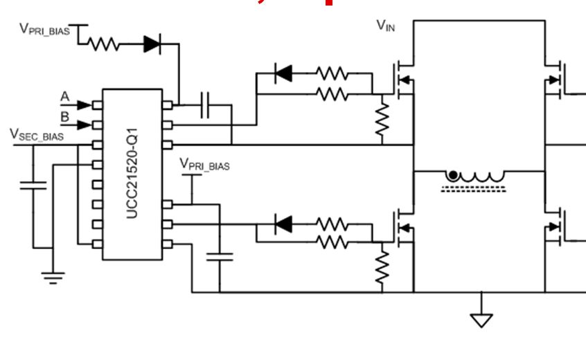
T2, T3: are basically the transformers used to isolate and scale the gate drive, TI has released much efficient isolated gate drivers which can replace these transformers, I suggest using UCC21520 which is a dual channel gate driver; you will need two of these for GATE A/B/C/D.
T7: is the Shim inductance which is based on the energy required to achieve ZVS. This can be calculated either from Equ 61 in UCC28950 datasheet or from the calculator attached.
when I am working with design sheet SLUC222C and generating file for specifications of PMP8740 designs i.e (Vin range: 370-390-410VAC, Output : 20-27-32VDC , Pout: 2KW, Fsw: 100KHz, effi:93%, transient voltage 0.6V) it shows shim inductance value as -ve and comment is "calculated LS is negative and LS might not be needed, leave a place of holder just in case" if it is so then why shim inductnace (T7) is connected in design?
also if we consider shim inductance value as 0uh then errors shown in input capacitance selection , current sense network selection, initial delay between ABCD section
If the Shim Inductance value is negative then you won't need an additional shim inductance because there is enough energy available to drive the ZVS transition. I will recommend leaving the cell with 0.5-1uH which is a negligible value (similar to what is done in the schematic) this cell should NOT be left zero.
The 4uH leakage inductance value sounds a reasonable assumption too.
The application of the isolated gate driver is relatively simple and straightforward. Please refer to the application guide and user guides attached below, this will help you to integrate UCC21520 with the design.
Please confirm in PMP8740
1. what switching frequency is used in DC-DC converter? are there different frequencies used for primary and secondary side calculations?
2. what is Duty cycle and Dtyp used in Dc-Dc converter?
Please explain how do you calculate values for L2 and Cin in PMP8740. L2 calculation is not given anywhere and if i calculate Cin as per application notes and datasheet of UCC28950 it gives different value. Please help.
can you share dc-dc main transformer details like no of turns of primary and secondary and wire gauge of both windings, so that i can compare with my design.
I have attached a paper that the designer of the product wrote, I would refer you to pages 10 and 11 for this case, the paper talks in depth about the inductor and capacitor calculations.
Regarding your previous questions: can you please be more specific about the white paper you are referring to.
As far as the transformer information: I will trust the calculator for the turns ratio calculations, we can not provide you with transformer winding details.
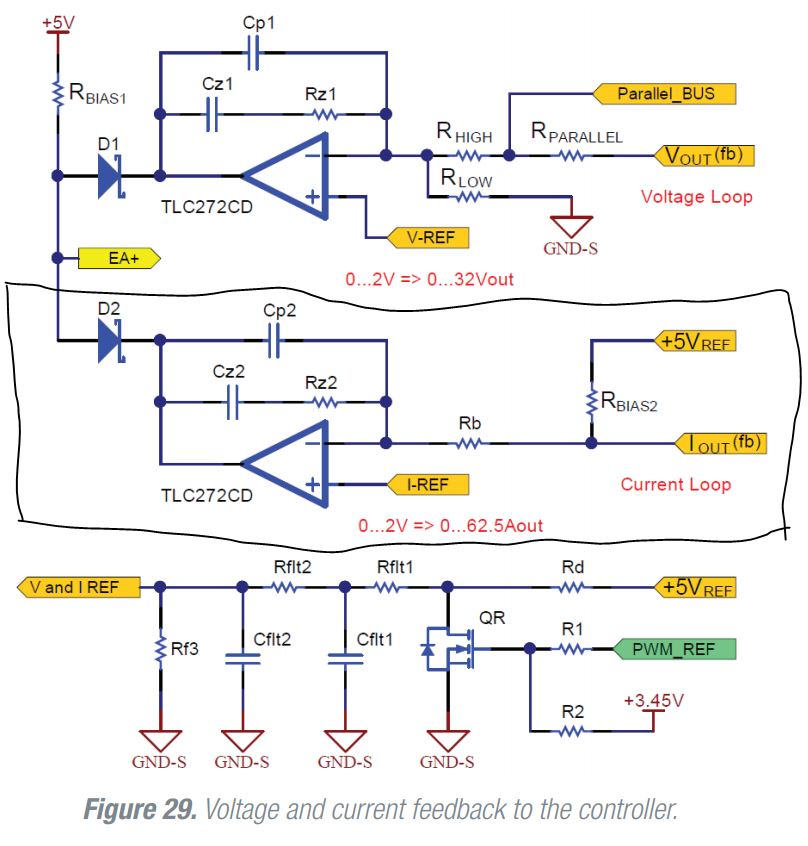
the Iout signal is used in the current loop alongside the voltage loop only to set the current limit, we cannot use the primary current signal for CI regulation because the primary current is a function of the input voltage and there is no fixed relation between primary and secondary current. This is why we need additional current error amplifier to set a demand level (EA+) for the control loop and so regulate the output current
For your second question, I do not understand it, can you please refer me to a text or a figure in the paper where you saw this. I might be wrong but I think you are talking about the parallel capacitors connected close to the output connector in figure 14, we use several parallel capacitors in order to better filter the output signal and eliminate the AC ripple.
I am refering " 2kW parallelable power supply module.pdf "
1)I am clear about fig 29 . voltage and current feedback to the controller, but please explain, in PMP8740 why this Iout signal used here in this voltage loop?
2) for your second question: sorry it was my mistake, my question was in PMP8740 design what is necessity of Q12, Q17, Q25-Q31, Q20 Mosfets in Output path? if I am not wrong, those all mosfets should be ON in healthy condition , also at start u-controller first check for reverse connection of battery to output terminal , if it is OK then turns On those MOSfets.
For the first question, R4 creates a positive output impedance and let Vout droop a bit in respect to Iout. This method helps to stabilize the parallel between modules when the battery impedance is very low.
The FETs are connected in parallel to reduce RDSon and looses when they are on. The reason for putting fets back to back is: when the converter is OFF the output capacitance is discharged. You connect a battery to output terminals and you charge these capacitors in zero time, and a spark will appear to the terminal, damaging them and putting stress on capacitors.
The FET Q17 is needed in case you connect the battery reversed, the body diode of the synchronous rectification FETs will be destroyed. By means of RT1, this current is reduced and this thermistor switches to high-resistance at high temperature. The microcontroller reads Vout and since it reads zero, will never enable all these FETs in series with the load.
If your system is a “normal” power supply and not a battery charger, you don’t need all these FETs.
I hope this answers your question.
Please hit Answered if you think your Question has been resolved.