This thread has been locked.

If you have a related question, please click the "Ask a related question" button in the top right corner. The newly created question will be automatically linked to this question.

UCC27714: How to slow HO rise time for NFET soft start cycles

Guru 55913 points
Part Number: UCC27714
Other Parts Discussed in Thread: TIDA-00778, TIDA-00909, TM4C1294KCPDT, UCC27712, , UCC21220, LM5170-Q1, DRV8301

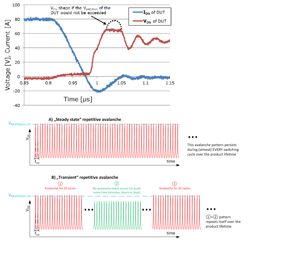
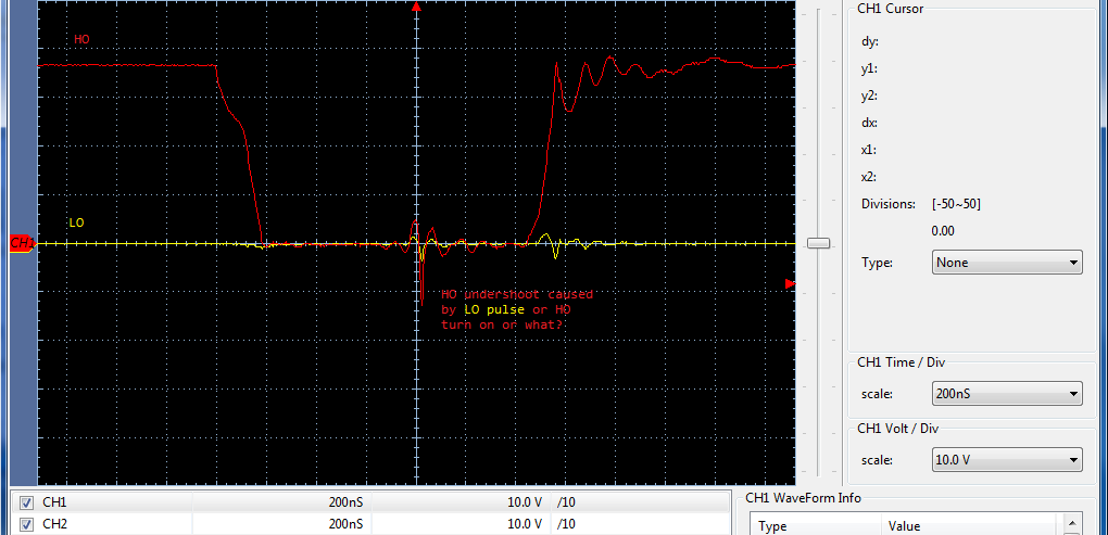
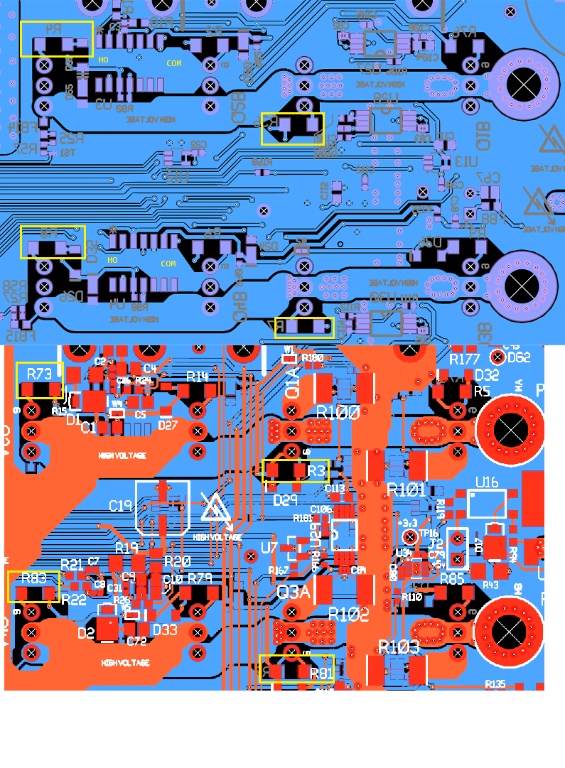
What can be done to calm 10Mhz ringing of HO output causing random very high VDS peaks? Is there some way to reduce HO output bias slowing the rise time other than adding excessive amounts of gate drive resistance or adding gate capacitance? It seems the flat top is more indicating of IAS events than we currently are seeing.

Adding gate capacitance seems counter intuitive to what TI documents are claiming about LS/LD/Q. Can the typical HO gate drive pull down resistor value connected to HS effect the HO output signal if it is to large in value? Why is there no mention of TI gate drivers HO output causing turn on oscillations when NFETS are being used versus IGBT modules? The problem is the source side voltage peak shown in captures can exceed VBR(DSS) at higher working voltages if left unchecked.

These voltage spikes seem much worse with the faster UCC and how much gate resistance is considered to much for small QG-NC values? Can COM pin tied to ground plane lead to high VDS spikes when digital ground is isolated from analog ground or COM? Note the HO output capture above is not consider avalanche being the top is not flat as shown below but it easily could enter IAS with higher working voltages exceeding VBR(DSS).


  • Hi BP101,

    Are you using 25V rated BVDSS FETs? I'm not sure if I asked you before, what FET p/n are you using?
  • Hi don,

    Don Dapkus said:
    Are you using 25V rated BVDSS FETs

    BVDSS=200V and when Bus voltage finally +165v easily be pushing IAS single pulse envelope! Sadly the next step up 80vdc is behaving badly in light of random source spikes.

    Was wondering if lowering +15 VDD pin to +12v  might help mitigate HO turn on 10Mhz ringing voltage spikes? The HV spikes club MCU locking it if they occur during heavy load at motor startup. There has always been some ringing with other gate drivers but the voltage spike peaks were small, typically less than 10v above DS. 

    Alternatively making Rgate 75 ohms might be the next value, so far larger Rgate values have produced less than good results.

    /cfs-file/__key/communityserver-discussions-components-files/196/7360.IRF-OptiMOS-200v-84amp-300watt-12mOhm-TO220-IPP120N20NFD.pdf

  • Hi BP101,

    I posted a reply about the decoupling capacitors on your other thread: e2e.ti.com/.../2580419

    Our device isn't capable of driving 10 MHz pulses, but your circuit could certainly have parasitic elements that can cause oscillations in that range. Many times I've seen power mosfets oscillate due to the RLC tank formed by the driver resistance, parasitic inductance, and the input capacitance of the power MOSFET. Due to their faster switching times, this is more common with mosfets than IGBTs.

    I always like to see a resistor next to the gate terminal of the power MOSFET to try and calm this tank circuit.
  • Hi Don,

    Don Dapkus said:
    I always like to see a resistor next to the gate terminal of the power MOSFET to try and calm this tank circuit.

    Perhaps a good thing Rgate is placed right next to the gate lead. The HO leads were kept very short in the parallel FET layout. Oddly HO oscillating (9-13.5Mhz) is far worse than LO which has much longer traces.

  • Hi BP101,

    It has been some time since this thread was addressed, and our conversation seems to be continuing in this other thread. Are you still looking for a reply on this thread? Please let me know.

    Regards,

  • It was Don that pursued the other thread, it was basically answered in my post lowering dead band time to 80ns. The other thread was vague mostly asking why ghost ringing was occurring HO/LO leading to very high pulse peaks.

    Our DC supply now 80vdc, HO driven NFET source pulse peaks reach 122v, very periodic / typical. In my opinion the rise time after Miller plateau is way to fast for NFETS with low QG-NC, perhaps below 100NC. The datasheet title seems to misrepresent UCC being good for NFET's, 4amp gate drive / motor drive, together they seem to be a bad combination when producing trapezoidal wave forms. There are no transients being produced by our PCB layout causing the UCC gate driver HO/HS to misbehave. On the other hand the UCC is procuring high voltage DC transients by it's HO/HS structures when producing trapezoidal wave forms.

    Perhaps reason enough TI LAB engineer/s should update datasheet maybe produce a work around in this case. Not saying other gate drivers did not produce ringing but others did not produce high VDS peaks that will exceed BVRdss at some point. Seems the UCC gate drivers were mostly tested with TI power supplies, PWM producing complementary HI/LI signals. Trapezoidal wave forms require center aligned PWM signals with overlapping HI/LI inputs of different duty cycles. That alone may be causing the HI input Schmidt trigger to pulse the HO totem pole for a longer period when it should not, unexpected errata!     

    TIDA-00909, TIDA-00778 both produce sinusoidal AC wave forms, of course major ringing is present in the GAN drive captures but the peaks are low. Not because the gate leads are short or fewer parasitic, rather the PWM switching signals roll off (sine wave) at HI/LI inputs are faster than that of PWM producing trapezoidal waveform. Both TIDA produce AC simulated wave forms, brings to question how TI LAB determined the UCC is even remotely compatible for trapezoidal digital motors? Has TI ever tested the UCC for producing PWM trapezoidal wave forms or did it simply assume that is could?

  • Hi Derek,

    These updated captures (80VDS) 12.5Khz shows rise time and magnitude of typical aggravate pulses being produced via trapezoidal wave form.  We use center aligned overlapping HI/LI inputs from three PWM generators  (TM4C1294KCPDT) to drive local 3 phase inverter as explained above post. Notice the only pulse that is never above VDSS is the very first pulse at the beginning of each trapezoidal wave form, code step 1-2. Reducing slew rate on HI input relative to LO slew rate makes no difference to the magnitude of pulses. It appears the UCC 1/2 bridges are attempting to boost the motors stator voltage as if it were a power supply. These HO drive high voltage peaks were not present in our PCB prototype using a much slower gate driver.

    Has TI produced another gate driver with same pin out that may correct this condition? Increasing HO drive resistance beyond 75 ohms seems an odd way to correct what seems to be trigger pulse errata that occurs when the PWM duty cycle on LI overlaps HI in the same 1/2 bridge, even with high dead band times and 1.6us minimum pulse widths. 

  • Hi BP101,

    Thanks for your patience in describing these issues. I don't think we ever tested the trapezoidal PWM case, and a lot of our testing was conducted with IGBTs which obscured a number of the behaviors you have described in the MOSFET case. UCC27714 is the only 14-pin gate driver in our catalog right now, and although we have a few other 8-pin 600V half bridge drivers such as UCC27712, they include 150ns interlock protection between HO and LO which wouldn't work with your system configuration. There are some isolated drivers, notably the 16-pin UCC21220, which could be adapted for similar functionality.

    Regards,
  • Perhaps TI could get TIDA-00778 engineer to write code to produce trapezoidal wave forms via UCC27714, the IGBT module (QG=275nc). Hard to imagine IGBT module would not produce similar results as above capture or worse being a saturated transistor back half.

    Center aligned HI/LI overlapping PWM duty cycle seems suspect leading to high random peaks in HO drive current, hence uncontrolled ringing/ripple current signature results HO output. Perhaps excessive holes flowing out/into the NFET gate region occur from excessive HO current gain. That would explain the uncontrolled random high voltage peaks produced via the NFET source and why larger gate resistor values on HO appear to slow down hole flow before single pulse IAS events occur. Obviously that latter method is not the WA we seek. If the UCC27714 has an errata condition, it would behoove all if made public in a disclosure PDF!

  • Derek Payne said:
    Thanks for your patience in describing these issues.

    Had to first understand what is happening relative to previous inverters with other 600v gate drivers not having same issue. That has truly stalled this project for a few months now besides other gotchas showing face.

    Derek Payne said:
    UCC27714 is the only 14-pin gate driver in our catalog right now,

    Perhaps we can put a band aid on it or at least understand why the series Gate resistance has to be made very large for Trapezoidal wave forms? Adding 10k across HS/HO versus 20k did help reduce the peak somewhat at 80 VDSS. The total QGNC will double for parallel NFETS. The primary goal was to prove the PCB was functional as an inverter motor driver before blowing the crap out of very expensive NFETS in the process. So far we have destroyed 5 UCC in the process but can not understand how the HO output was compromised with the very same pulse widths we are using now. Oddly HO is not shorted to HS or HB or HS to COM/VDD pins.  

    Derek Payne said:
    There are some isolated drivers, notably the 16-pin UCC21220, which could be adapted for similar functionality.

    Ok and do now see secondary pulses (typical) perhaps HI Schmidt pulse shaper becomes slightly saturated making Totem poles drive current accelerate HO gate drive. That is why 16.0v zener across HO/HS near each NFET has no ability to control current each inductive ringing cycle that occurs after. The demagnetization primary pulse is the only high pulse that stays even to 80 VDSS which occurs after HI has not been fired by 120 electrical degrees.

    Below is capture of the Trr recovery occurring along HS or ground. The center pulse caused by duty cycle @24 VDSS dead band time. Now at 80 VDSS had to make dead band 120ns and 1.6-1.8us minimum pulse width to stop over current fault conditions but that center pulse is not occurring at faster duty cycles. Basically HO turn off Trr is very clean (heal), hardly produces any (di/dv/dt), such makes the UCC superior in that regard.


  • Little dity below technical note: Shorter dead time effecting Qrr/Trr recovery was spot on and 80ns dead time removed di/dt negative undershoot pulses of Qrr.

    - Body diode conduction usually happens during dead time; therefore, it can be reduced by minimizing the dead time. However, there is always a limit how low the dead time could go down to.

    - Diode conduction current is often set by the chosen topology, and changing topology is normally not desired.

    Current slope (di/dt) is related to the parasitic inductance of the commutation loop. First, it would require a redesign of the PCB to improve Qrr. Second, a low di/dt means large parasitic inductance, which usually contradicts to a good PCB layout for high frequency application.

    Our PCB UCC footprint has virtually NO Qrr/Trr undershoot with the improved OPTIMOS-FD devices. 40% reduction in Qrr has significant efficiency benefits! Sadly improved Qrr can not slow down inductive inrush current shown in Trapezoidal waveforms VDS peaks that HO drive slew rate appears to aggravate.

  • Hi BP101,

    What else do we need to do on this issue?
  • Hi Don,

    It seems Derek gives good example why TI bench has not produced PDF of workarounds for high VDS peaks. If the bench considers the time period after Miller 2 the NFET Qrr recovery that would explain a lot. It only recently became very clear the high peak VDS is result of inrush current into the inductor.

    That peaking does get a little less at higher VDS supply but does not entirely remove the condition requiring very large gate drive resistor value on HO output. Perhaps why TIDA-00778 engineer added 2200pf caps on the HO/LO gate drives but never states why that was done in analysis section. No PDF explains why adding capacitance on the NFET gate is even required by the gate driver! if there is a workaround for adding capacitors to the NFET gate it should be documented somewhere, right?
  • Hi Don,

    It seems I was not to far off in asking about soft start UCC27714 HO drive as being implemented on LM5170-Q1 Multiphase Bidi current controller. Have a look at figure 63, soft start cycles driving the NFETS.

  • Hi BP101,

    Hmmmm, I'm having trouble finding your reference. I can't find a Figure 63 in anything I'm looking at.

    But, I do see mention of soft start in there. This is usually done by the controller upstream of the gate driver. It would be difficult for us to implement such a feature in our driver. Could you implement it in your software?
  • Hi Don,

    Figure 63 in the LM5170-Q1 datasheet page 57.

    Yet the  DRV8301 produces Idrive cycles, Fig. 11 gate drive current control section. Soft start current cycles can not be done via software as the HO Totem pole current drive must be controlled at the gate driver level. There is also Wiki page discussing how gate driver controls NFET GS current hold steps to prevent shoot through. Of course these types of gate drivers are low voltage devices but they are evolving motor drive technology.  

    7.3.5.2 TDRIVE: Gate Driver State Machine

  • Sorry that part number was typed backwards, astigmatism correction do that all the time.
  • Hi BP101,

    No problem, I feel your pain with regards to your eyes.

    I still suggest it would be difficult for us to put soft start in a part like UCC27714. this is a building block part, very generic in nature, and I don't think most customers would appreciate the outputs doing something different than what they are inputting to it. Those other two parts are for specific use cases, so they can include soft start in them.

    I'll bounce this off my colleague to calibrate me, I'll let you know if he agrees.