This thread has been locked.

If you have a related question, please click the "Ask a related question" button in the top right corner. The newly created question will be automatically linked to this question.

TPS55165-Q1: Can not get reated power output

Part Number: TPS55165-Q1
Other Parts Discussed in Thread: TPS62160,

The design target of this non-isolated dc/dc is:

input : 8~32Vdc;

output: 12Vdc 800mA;

For the Same schematic, i have 3 PCBs in hand and only one of them do work well.

1. The demo PCB. Made it about half year ago to try this chip. This PCB is working well, can output over 950mA @ 12Vdc, (input:7~32Vdc);

2. The prototype of my Product. a little big different of PCB layout. Does not work, i have details below.

3. The compare/fix PCB. To make the prototype board work, made another small PCB just for this aux power supply to try to fix it. change a little bit of layout based on first demo PCB and example from Ti. Still not work.

The 2nd board test detail.

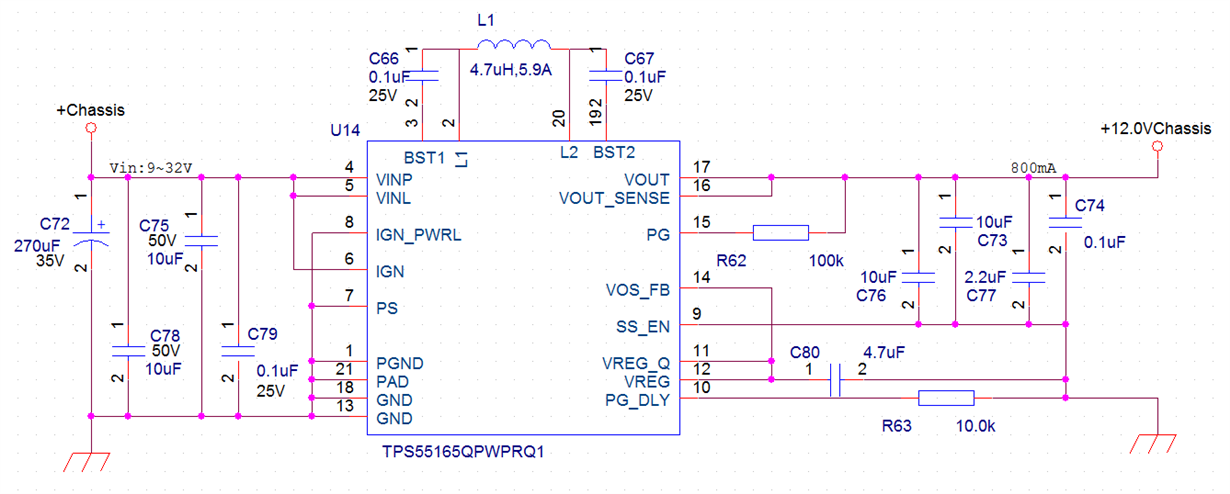
Schematic.

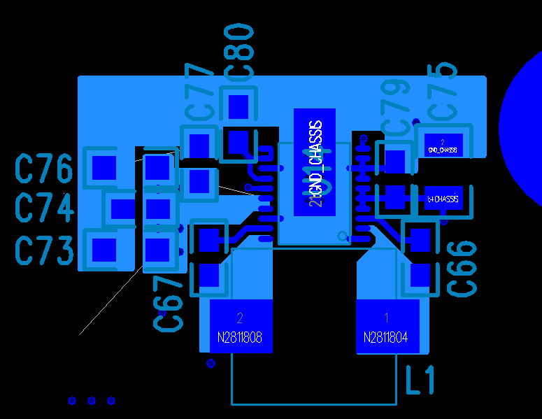
PCB layout.

it's a 6 layers PCB, and the layer next to the components is GND.

BOM

Reference

NuGen Part Number

Description

Manufacturer

Part Number

C72

230-N277C350HYP-000

Capacitor, Hybrid Polymer, 270uF, 35Vdc

United Chemi-Con

HHXB350ARA271MJA0G

C75

230-N106C500X7R1210

Capacitor, Ceramic, 10uF, 50V, 1210


C78

230-N106C500X7R1210

Capacitor, Ceramic, 10uF, 50V, 1210


C79

230-N104C250X7R0805

Capacitor, Ceramic 0.10uF, 25V, X7R, 0805


C66

230-N104C250X7R0805

Capacitor, Ceramic 0.10uF, 25V, X7R, 0805


C67

230-N104C250X7R0805

Capacitor, Ceramic 0.10uF, 25V, X7R, 0805


L1

230-001253-047

固定电感器 XAL5030 AEC-Q200 4.7 uH 20 % 5.9 A

coilcraft

XAL5030-472MEB

R62

230-N1003R0805

Resistor,0805,100k,1%


C76

230-N106C250X7R1206

多层陶瓷电容器MLCC - SMD/SMT 10uF 25V X7R 1206


C73

230-N106C250X7R1206

多层陶瓷电容器MLCC - SMD/SMT 10uF 25V X7R 1206


C77

230-N225C250X7R0805

多层陶瓷电容器MLCC - SMD/SMT 2.2uF 25V X7R 0805


C74

230-N104C250X7R0805

Capacitor, Ceramic 0.10uF, 25V, X7R, 0805


C80

230-N475C160X7R0805

Capacitor,Ceramic,4.7uF,16V,0805,X7R


R63

230-N1002R0805

Resistor,0805,10k,1%


U14

230-001251

开关稳压器 2~36vin, fixed 12vout 0.8A

Texas Instruments

TPS55165QPWPRQ1

Test Result:

@ no load.

  the output Voltage is good for 8~32Vdc input.

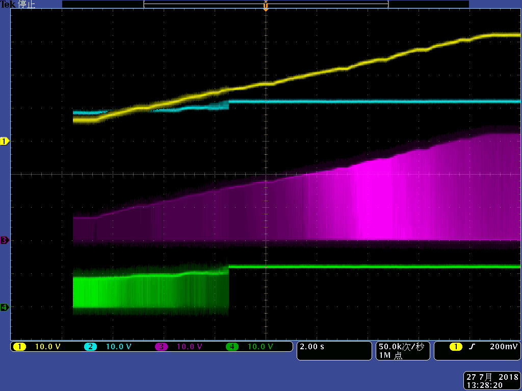
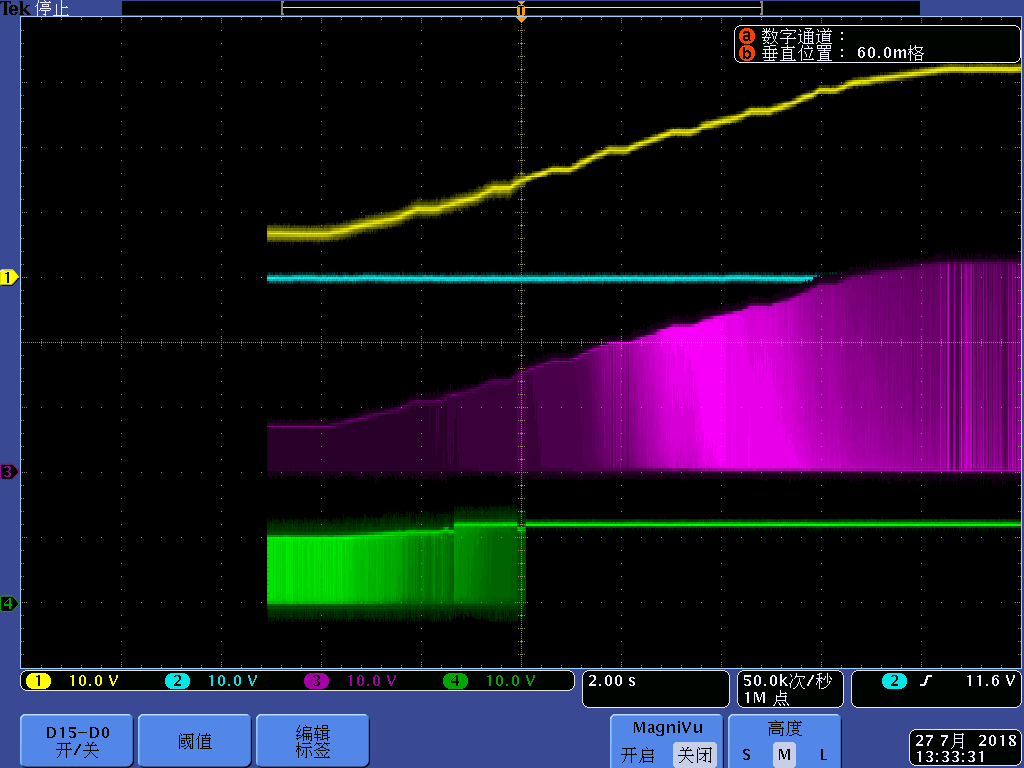
@ 20ohm load(about 400mA )

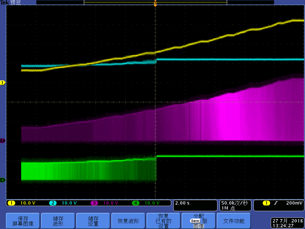
Yellow:input Voltage Vdc;

Blue: output Voltage Vdc;

Violet: U14.2 Voltage The left(input) side of inductor

Green: U14.20 Voltage , The right(output) side of inductor 

The pic below is noload

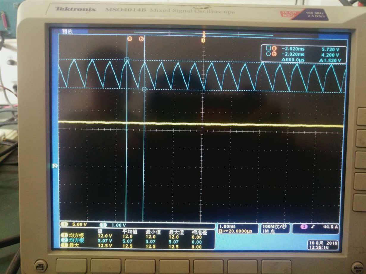
By Adding another 270uF HYP cap at output side can help a little bit of ripple, but does not make things working well.

See below 

With additional 270uF HYP cap at output side, 20Ohm load.

3rd PCB.

trying to make as close as the Ti example, within 2 layers (1.6mm) , which is even worse than 2nd PCB. 

  • Hi Sir,

    What is your original demo PCB?  how many layers do you use? Since your output power is big compare to the IC's maximum output capability. So at least a 4-layer pcb should be used, and should pure a very big copper plane and use at least 2oZ copper thickness.

  • Hi Helen,

      Thank you for your help.

       to make things clear, i have attached the detail of PCB and Schematic for all 3 boards i have here.

      Question:

       1. can you help me find out what the reason or biggest effect for this DC/DC when changing the board layout one to another.

       2. from the cost request, we can only do 2Oz copper on top and bottom layer, 1Oz copper for all inner layers, is that good?

      3. i am going to drawing the 4th PCB as a single DC/DC module to put on my product board, can you help me to verify my drawing?

      4. how important to separate the output cap from a 22uF to 10+10+2.2uF?

    Thanks and best regards.

    Bing Xie

    TPS55165 PCB details.docx

  • Hi Helen,

    One thing forgot to ask,

    My biggest question is why the 2nd PCB( Product) doesn't work ,which have very similar Layout to the Demo board and Example Layout from TPS55165 data sheet?

    Thanks and best regards.
  • Hi Sir,

    one thing want to confirm with you. At what input voltage does this issue happens?  The maximum output capability at Vin=8V is only 0.6A.

    Is there any output capacitance difference between the three version pcb board?

  • Hi Helen,

    Thank you for your quick respond.

    1. the request is input between 9~32Vdc, output 12Vdc 800mA.
    2. If you looked at the Schematic, you will see, the demo board is using 2 of 22uF caps, and later boards are using 2 of 10uF with 1 of 2.2uF.
    I have try the following steps, but doesn't change the result.
    i. change the demo board output cap from 0.1uF + 2x22uF to 2.2uF + 2x10uF. Still working well.
    ii. change the product board: from 2x10uF +2.2uF to 2x10uF +2.2uF +270uF(HYP). Still not working well.
    the output voltage is lower than 12Vdc until input voltage increased higher than 15~16Vdc(Pure buck mode, see it on o'scope screen pics) with 20ohm load( which means about 450mA under 12Vdc output , and less current when output voltage does not meet 12Vdc).
    Thanks and best regards,
    Bing Xie.
  • Hi Sir,

    Since your output current is rather big, so please use at least 2*22uF cap at the output side. Be ensure its effective output capacitance is much  higher than 2*10uF cap.

    Another question is : Did you guard the input current or the inductor current. In the boost mode, the Input current should lower than 1A? Did you have input current dada during the test?

  • Hi Helen,

    for the output cap, OK. the reason to reduced to 2x10uF is based on data sheet suggest. it's ok to put 2x22uF and have a try.
    will provide test result to you later.

    for he demo board, at about 7~8Vdc input ,with 10Ohm load( 12Vdc output , about 950mA), the input current is higher than 1A, and system still working well.

    i do not have tool to measure the inductor current.

    the sat current for inductor is 5.9A. just FYI.


    Thanks and best regards,
    Bing Xie
  • Hi Bing,

    Then what is the input current for your un-work board at Vin=10V, Vo=12V with 20 ohm load? you can read it from your DC power supply I think.

  • Hi Helen.

    I did a test with the config that all 3 boards have same output cap config, 2x10uF + 1x2.2uF.
    The test result is :
    The Demo Board: can keep around 950mA output at 12Vdc( 20 Ohm load) , the input voltage range is 8~32Vdc. the output capability is greater than data sheet at 30C room temperature.
    The Product Board with 10Ohm load can only provide 12Vdc output when input voltage is higher than around 15~16Vdc. You can check the O'Scope pictures i post in the first question.
    The Mini Dc/DC board(3rd), worse than the product board. the output voltage could drop to 0V even without any load for uS level.
    Thanks and best regards,
    Bing Xie
  • Hi Xiebing,

    Please tell us the input current at the boundary of the normal working. Input current is very important at boost mode.  Please decrease the load to a value when it can work normally then detect the input current, this will help us to determine the problem.

  • Hi Helen.

      The following test has done for additional information.

    1. Set the Demo board output cap to 2x10uF + 1x0.1uF. does not change the output capability compare to 2x22uF + 1x0.1uF. it's working with 1.15A loads at 12Vdc output with the input range from 8Vdc to 32Vdc.

    2. The Mini DCDC Board(3rd) does not work with the same config as the test above. the output drop to 0V for about 20mS often without any load with the config of 2x10uF + 0.1uF output cap.

    3. Test the Product Board which better than mini DC/DC but not really working.

    *Note: besides the resistor load i put on output side, there are other components liek resistors, OPAMPs and some small DC/DC like TPS 62160 exist, which will use some power.  I have done the test, (take off the inductor of TPS 55165 making this DC/DC stop, wiring a power source to the output side of TPS 55165 directly and record how much current are request when we have so call NO LOAD)

    Vout Iout
    V A
    5 0.03
    6 0.04
    7 0.035
    8 0.055
    9 0.08
    10 0.08
    11 0.08
    12 0.085

    The following test result is what you request, the input current of TPS55165

    Load 40 Ohm  
    Vin Iin Vout Iout
    V A V A
    6 0.57 9.25 0.221
    7 0.51 9.68 0.231
    8 0.44 9.85 0.234
    9 0.41 10 0.24
    10 0.39 10.1 0.242
    11 0.34 10 0.239
    12 0.33 10.6 0.252
    13 0.32 10.6 0.253
    14 0.31 10.9 0.26
    15 0.31 11.4 0.272
    16 0.32 12.1 0.289
    17 0.3 12.1 0.289
    18 0.28 12.1 0.289
    19 0.27 12.1 0.289
    20 0.26 12.1 0.289

    Load 200 Ohm  
    Vin Iin Vout Iout
    V A V A
    6 0.27 9.77 0.045
    7 0.24 10 0.047
    8 0.21 10.4 0.048
    9 0.2 10.8 0.051
    10 0.18 11 0.053
    11 0.16 10.7 0.05
    12 0.17 12.2 0.058
    13 0.16 12.2 0.058
    14 0.14 11.7 0.056
    15 0.14 11.3 0.054
    16 0.13 12.1 0.058
    17 0.12 12.1 0.057
    18 0.12 12.1 0.057
    19 0.11 12.1 0.058
    20 0.11 12.1 0.058

    Load   No load*  
    Vin Iin Vout Iout
    V A V A
    6 0.21 12.2 0
    7 0.18 12.2 0
    8 0.16 12.2 0
    9 0.16 12.2 0
    10 0.12 10.9 0
    11 0.12 11.3 0
    12 0.11 12.1 0
    13 0.104 12.2 0
    14 0.1 12.2 0
    15 0.14 12.2 0
    16 0.09 12.1 0
    17 0.09 12.1 0
    18 0.09 12.1 0
    19 0.09 12.1 0
    20 0.09 12.1 0

    Please let me know if you have any questions,

    BTW: where are you? are you a Chinese?

    Thanks and best regards,

  • Hi Helen,

    A quick question.

     I am drawing the 4th board which seems like the 3rd board(mini DC/DC board) using the suggested 4 Layers board.

    Based on the cost request, can i just use 1 Oz for Copper?

    and here is my Layout File in PDF, can you help me to check the layout?

    Top Layer:Trace and Copper.

    2nd Layer:GND

    3rd Layer:Vout(12V)

    Bottom Layer:GND

    to Reduce the total debug time, i'd like to make another PCB very quick, that i can test by next Monday.

    Thanks and best regards

    Bing Xie

    040-000208-a00 rev - evc403-xx8.pdf

    GWK1.pdf

  • Hi Bing,

    The schematic is OK. But I can't check the pcb as it is in black and white.  Could you please convert the pcb layout to colorful one?

  • Hi Helen,

      I have couple different format of the PCB file attached.

      please let me know if you can open it or not.

    if possible, please let me know which format is easy for you to read.

    I am using pads 9.5 to do the layout work.

    Thanks and best regards,

    Bing XiePCB file in different format.zip

  • Hi Helen.

    Forgot to share you that the demo board is a 4 layer 1Oz in each layer board.

    the layout see this attach022-000211 Rev X1 Buckboost pushpull flyback powersupply demo bd.pdf

  • Hi Helen,

      Just get some ideas.

        I think the reason for 4Layers board, one thing important is the impedance of the PCB.

    The Demo 4 layers board using typical structure which means it's only a 5mil 2116/7628 between top layer and second layer.

    The product board i made is 2.4mm 6 layer even thickness board structure which mean there are 17.523mil (2116+2116H+7628) in betweeen top layer and second layer, which increased the impedance between top layer and second layer.

      and for those high frequency switching power devices, the impedance is very important.

      and this explain that why 2 layer 1.6mm board does not work even without any load.

    is the understanding above correct?

    Thanks and best regards,

    Bing Xie

  • HI Bing,

    1.6mm board should also be OK if the layout is good and the there's no damaged component . I'm wondering if there's some component is damaged? and whether  you use  a high frequency inductor. ferrite inductor is not fit here.

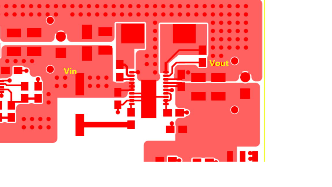
    Confirm one thing with you, is my understanding of Vin, Vout right regarding the following picture?

  • Hi Helen,

    1st your understanding of the layout is correct.

    2nd.

       I just found something new today, which make me believe the spacing of top layer and second layer is the critical point of making high frequency switching power supply.

      in the product board, there is another DC/DC exist based on TPS62160, to convert 15 V to 3 V, which has tested and passed before.

       Now it's have the issue of

        A. a lot of Vout Ripple without load

      B. under 245mA load, it's still output 4.95V, but the voltage drop to 3.14V @ 302mA.

         And i have the same Schematic and layout in another board which is 2.4mm 6 Layer board, has only 7.337mil spacing between top layer and second layer, the DC/DC ( tps62160) working well at that board.(Tested up to 725mA without voltage drop).

      So i think the spacing between top layer and second layer( gnd) is very important for this switching power supply.

    I am modify the layout to 4 layers , put another issued DC/DC together(tps 62160) and targeting is release the board in 12 hours.

    Please let me know if you have any questions,

    thanks and best regards.

    Bing Xie

  • Hi Bing,

    It looks that the circuit is disturbed by the noise signal or there's something wrong with the load current? Could u confirm that all the other load have been completely removed, there's no other load eat an extra amount of current?

    If it is because of the noise issue, then did you test the SW1 and SW2 waveform of the TPS55165-Q1, is the SW waveform stable? what is it looks like, you can use 400ns/div or 1us/div to check it.   Please check carefully on the original good demo board. Is there any difference on the layout, each function circuit's placement? Is there a whole unbroken GND plane at the inner layer?  a whole unbroken GND plane at the inner layer helps to isolate the noise from the back side.

    If not because of the noise reason, then did you change any component comparing to the demo board?  Is C11 connect well, where is it? what is the size of it. The circuit can't work well if it is too far away from the IC or its size is too small which leads to small effective capacitance.

  • Hi Helen,

      Thank you for your help.

    I have fix this issue.

    With the same layout, just increase the layer to 4 ( 4 layers 1Oz PCB), and reduce the spacing between top layer and second layer from about 17mils to about 5 mils make the chip back to work.

    I think the independence is the core of the feedback look of those chips( TPS55165 TPS62160)

    Again , thank you for your help.

    Valve Xie 

  • Hi Bing,

    Thanks for the update. What is your second layer, is it a whole unbroken GND plane?

  • Yes.
    The second layer is a whole unbroken GND plane.
    the core is how far away from the GND plane to the top traces.
  • Thanks Bing.

    Then is there any noise circuit at the back side of TPS55165? how did you connect Vo-Sense, is it connect with Vo pin directly? Vo_sense is sensitive.

  • Here is the layout. the Vout are came from mian output cap (10uF x 2) and have a 0.1uF to do decoupling , then feedback to chip.

  • Hi Bing,

    The layout for the Vo_sense part is OK. Then what is the trace at the back side? Is there any noise trace at the back side?  The TPS55165 EVM board its top layer and the second layer is 15mil distance and there are 3-layers GND copper plane.

  • The 3rd plane is Vout and Bottom is empty.
  • Suggest you pour the 3rd layer and the bottom layer with GND copper plane if possible.
  • Why doing that? i mean with the GND in the second layer, the system is working . Is there anything i missed?
  • Multi layer GND coper plane is good for the noise sensitive circuit. But anyway, its up to you since your new board is also worked.