This thread has been locked.

If you have a related question, please click the "Ask a related question" button in the top right corner. The newly created question will be automatically linked to this question.

WEBENCH® Tools/LMZ20502: LMZ20502 failed to regulate

Part Number: LMZ20502

Tool/software: WEBENCH® Design Tools

Dear Forum,

I am having issue with LMZ20502 and I hope to get some ideas/suggestions as what could be wrong with my LMZ20502's circuit.

I used the WEBENCH DESIGNER to obtained the circuit for LMZ20502 with 3.3V input and output is 1.35V. The problem I am running into with this circuit that the output started out at 1.2V and it kept rising upto 1.6V and sometimes it got up to 2V. The WEBENCH recommended a 47uF/10V cap and output cap of 22uF/10V. The the feedback pin FB, I used 69.8k and 56k to obtained the Vref voltage at the feedback pin FB.

Thank you in advance for your input,

BR,

Howard

  • Hi Howard,

    My apologies for not getting to your thread. Can you share the Webench design you generated if you have it?

    Regards,
    Jimmy
  • Hi Howard,

    Is this the Webench design you used to create the schematic and PCB for your board?

    Webench Design: webench.ti.com/.../SDP.cgi

    Regards,
    Jimmy
  • Hi Howard,

    Do you have any update on this? If you look at my shared design schematic, does this match what you have on your board. I don't think there should be any issue with the component selection that Webench designer recommended since simulation is created using experimental data driven tests.

    Regards,
    Jimmy
  • Hi Jim,

    I am sorry for not getting back with you earlier. Attached please find the schematic page for this part.

    Thanks,

    HowardLM20502.sch.pdf

  • Hi Howard,

    Can you provide a waveform of Vin,Vout, FB and PG for me? Also what loading do you have when you see the output voltage drifting? Normally Vfb should be 0.6V and with your resistor divider option provide a stable Vout of 1.35V.

    Regards,

    Jimmy 

  • Hi Howard,

    Can I get an update on my questions above? Also if the problem is still there, can you try to lower the resistors so there is a stronger pull down current at 1.35V. Perhaps a 35k(Rtop) and 28k(Rbottom) feedback resistor set.

    Regards,

    Jimmy 

  • Hi Jimmy,

    We had to send the boards out to replace the LMX20502s. We have three boards with the same failures. We replaced the LMZ20502 chips on all three boards, and two are now working and one still fails. We have a few questions that we need your help understanding them better.

    1. This part is starting up in a pre-biased rail. A blog on the TI web site that stated the part is not guaranteed to handle the pre-biased scenario. Can you comment on this?

    2. Can you explain more about the MODE pin (PFM vs PWM)? Would this play a roll in the failure of LMZ20502?

    3. Output capacitance - section 8.2.1.3 Output and Feed-Forward Capacitors, notes that "The maximum value of total output capacitance should be limited to between 100μF and 200μF." Does this include the load capacitance (bypass and decoupling caps) at the chips or just the output capacitors right at the output of the LMZ20502.

    4. EN - We suspect that the buffer which drives this signal might not be powered when the LMZ20502 is powered up. In other words, EN might be floated. 

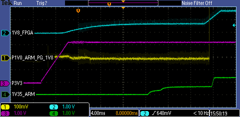
    5. The pictures attached are from a successful power up of the board that failed and was replaced with a new LMZ20502 chip:

  • Hi Howard,

    1. Can you attach the blog for reference?

    2.PFM and PWM operations are thoroughly explained in section 7.4.1 and 7.4.2. But to answer your question, PFM mode only really kicks in at light load where the switching frequency is modulated. This mode helps with power conservation at light load since the converter will shut down if it detects the output voltage is at the voltage reference threshold, meaning the power supply doesn't have to pull much current at this point. In your schematic, it looks like the device is sinking 2A which is way above the light load range. I don't think this is why the regulator is not working in your application.

    3.The maximum effective output capacitance range detailed in section  8.2.1.3 is for the entire capacitance seen on the output of the regulator. This accounts for the output capacitors local to the regulator and any other downstream capacitance from either FPGA or other circuits. 

    4. Please ensure that EN is pulled high. It is not recommended to have the EN pin in tri-state/ floating. This is one of the things that is listed on the Do's and Don'ts in section 8.3 

    It might be worthwhile for troubleshooting to pull EN to VIN(always on operation) and perform a loop stability test and startup test at no load and full load. This should help narrow down if the issue is EN pin related or output capacitance related.

    Regards,

    Jimmy 

  • Hi Howard,

    Please let me know if you still have further questions on this.  If this is still a problem and you see this on multiple units, I recommend sending them into TI for failure analysis at this customer return link.

    Regards,

    Jimmy