This thread has been locked.

If you have a related question, please click the "Ask a related question" button in the top right corner. The newly created question will be automatically linked to this question.

BQ24296M: What could cause the SYS-GND resistance to decrease to ~1Ω (while powered off) after use?

Part Number: BQ24296M
Other Parts Discussed in Thread: TPD1S514, BQ24296

Hi all,

I'm using the BQ24296M IC in a charging circuit design. I noticed that the resistance between the SYS output and GND started in the tens of kΩ and slowly decreased to ~0.8Ω currently as the board was powered (no battery connected, VBUS = 5V). The resistance is measured when the board is powered off. This occurred over ~1-2h of total powered-on time while I was testing other parts of the circuit. The low resistance triggered the overcurrent protection, SYS fell to 0V and the LEDs (STAT and PG) turned off. Before completely dying, the LEDs behaviour degraded (randomly flickering and being dim). Needless to say that the IC is destroyed.

Furthermore, I noticed that the resistance between SYS and BAT (essentially the resistance of the BATFET MOSFET) also decreased; to around 66Ω this time. I believe that this mostly happened while a cell was connected between BAT and GND, but I cannot say with certainty. In addition, I noticed that the SCL, SDA and CHARGER_INT pins were not pulled to 5V as they should from the pull-up resistors. This indicates that (at least some parts of) the internal circuitry was also shorted/destroyed in the process, which pulled these pins down to ~0-1V in my case.

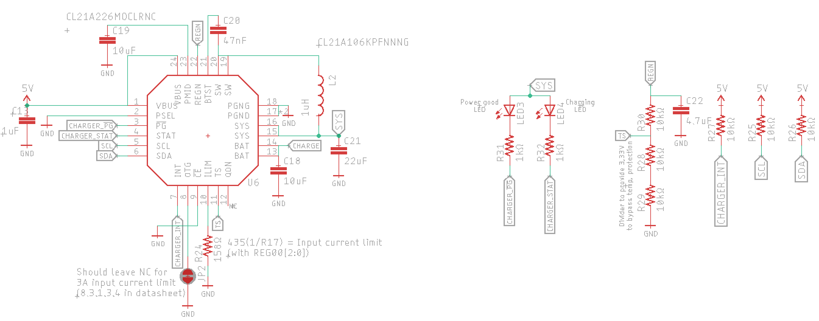
I can say that no cell was connected for 90-95% of the time for which the board was powered (as I was testing other circuit sections, not related to the BQ24296M). Also, the IC never got hot and no external components were damaged. This behaviour happened with two chips. Below is the circuit schematic. The CHARGE signal is connected to the Lithium-ion cell's cathode through a relay. OTG is no-connect.

Does anyone notice a schematic error which could result in the chip slowly destroying itself?

Thank you very much,

Tristan

  • Tristan,

    The schematic looks good to me. For the layout, the loop of Cap C19, PMID and GND should be minimized as discussed by the layout guideline on the datasheet page 42. Adding a X7R 1nF 0402 ceramic cap on PMID in parallel to C19 helps the EMC performance.

    BQ24296M SW rating is 7V max for normal operation. Depending on the characteristics of the adaptor, it is possible that the input voltage source has transient event exceeding the maximum rating during the operation and damage the low side switching FET Q3. To prevent the damage due to the input voltage stress, low voltage OVP IC or TVS diode with fast response time and accurate breakdown voltage for VBUS such as TPD1S514 can be used.

    During development or manufacturing, it is common to use DC source instead of battery for evaluation. However, care must be taken to ensure DC source has good transient characteristics during power on, power down, load transient. Care must be taken to minimize cable wire between charger BAT pin and power source or connecting a battery.
  • Hi Eric,

    Thanks for your answer. All design guideline have been respected so I doubt that would be the cause. I replaced the chip with a new one and ensured that a battery was connected at all times when the BQ24296 was powered on. It now charges correctly, following the default register parameters. In my design, there is no load on the SYS pin, so the switching regulator is not powering anything (unless charging the cell through the BAT pin).  Could it be that the absence of a load on the SYS pin produced switching transients that damaged the chip over time?

    Right now, I added a ~130Ω load resistor on SYS (to GND) to provide a load for times when the battery is either fully charged or mistakenly disconnected. So far, I haven't seen the same problems as before! I'll report back if I see anything else with further testing.

    Thanks,

    Tristan