This thread has been locked.

If you have a related question, please click the "Ask a related question" button in the top right corner. The newly created question will be automatically linked to this question.

BQ76200: BQ76200 can not load

Part Number: BQ76200

Dear Sir/Ms.

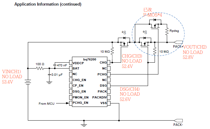
This is a problem encountered by my customers. CHG_EN, DSG_EN, and CP_EN all have HIGH signals. The measurement voltage is as shown below in NO LOAD.

but the customer only pulls 0.1A Load, and the whole voltage goes down. The DS0005 is shown as a pull-up. Please refer bellow picture.

I would like to ask what is the problem? Is there any way to improve it?

Best Regards,

Kami Huang

  • Hi Kami,
    The schematic segment included is a circuit option to provide a pre-discharge feature to bring up the PACK+ voltage of a high capacitance load to normal or near normal before turning on the discharge power FET to avoid a short circuit from the BMS. Note that the illustrator used an N-channel symbol rather than the intended P-channel symbol for the pre-discharge FET, so gate and source are swapped to keep the diode in the proper orientation.
    From the waveforms it looks like the pre-discharge circuit was not used or did not work as intended possibly due to the symbol confusion. Each attempt to turn on results in pushing up the PACK+ (VOUT) voltage. When full voltage is achieved the cycling would stop, but this is not shown.
    The loaded waveform shows more dramatic signal swing as the load depletes the charge on PACK+ between turn on attempts. There are 2 possibilities:
    1. Check the use of the pre-discharge circuit timing, be sure it is wired correctly and is on long enough to charge the load capacitance.
    2. Check if the BMS is seeing short circuit. You indicate DSG_EN is high, but check for drop-outs. If not the cycling may be caused by the bq76200 driver being pulled into UVLO. See the application note www.ti.com/.../slua794 and check the full schematic of the application. Check:
    The PACK pin is connected to the PACK+ with a small filter time constant.
    The PACK pin capacitor should be 10 nF or smaller.
    Be sure a suitable gate resistor is provided between DSG and the FET array. The FETs must bring up PACK+ without dissipating the CVDDCP into the PACK pin capacitor or leakage paths.
    Including the zener and resistor between DSG and PACK can avoid internal leakage paths.
    The discharge gate load must be within the capability of the charge pump. A 10M as shown in the schematic is suggested. Adding smaller resistors at each parallel FET gate-source can overload the charge pump.
    Be sure the CVDDCP capacitor was sized for the multiple FETs.