This thread has been locked.
If you have a related question, please click the "Ask a related question" button in the top right corner. The newly created question will be automatically linked to this question.
To whom it may concern.
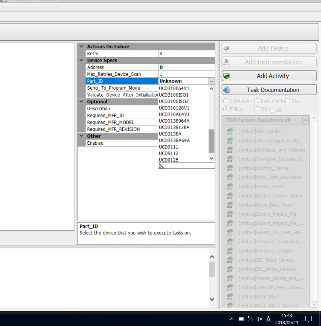
We are now trying to write software to UCD 3138, however we cannot write with Error message.
We are using the tool, TI Digital Power Production Tool, Ver. 2.0.9.
Even if we configure Factory Script according to the help, the following error message is appeared when pushed start after the road has completed.
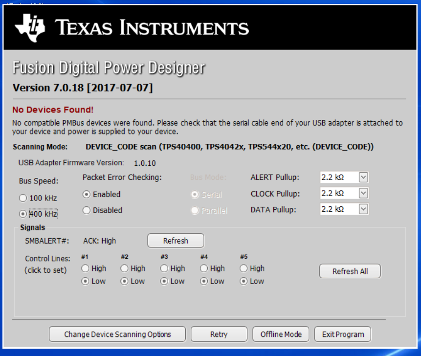
“Device UCD3138A@address XX was not found.”
We do not know how to set the address and cannot set the address.
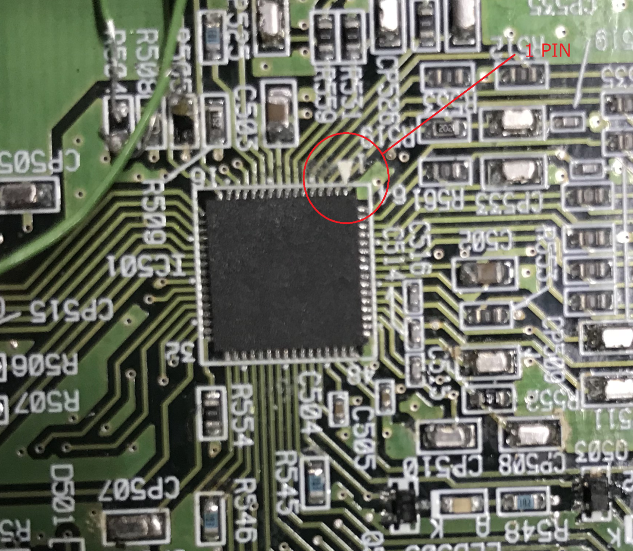
Is there a unique address of UCD3138RGCR?
Is the tool correct with TI Digital Power Production Tool, Ver. 2.0.9?
The current operation confirmation progress is shown below.
1.We confirmed if we could run the IC using Fusion Digital Power Designer which is used at evaluation circuit board UCD3138PSFBEVM0-027.
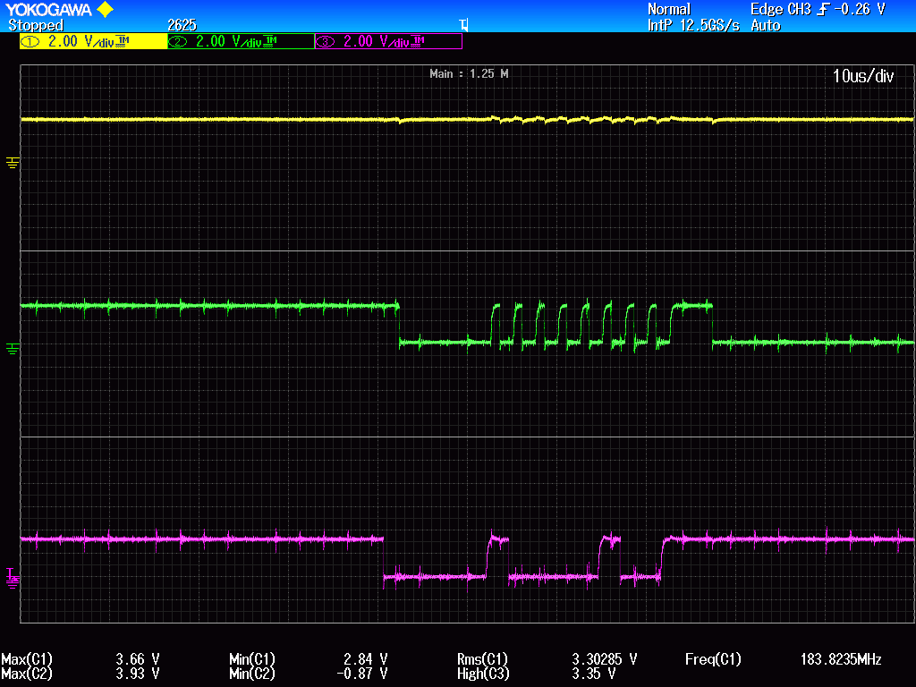
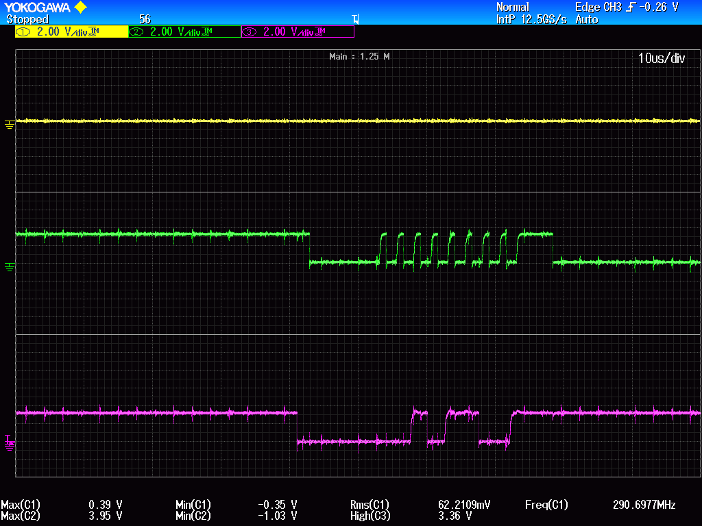
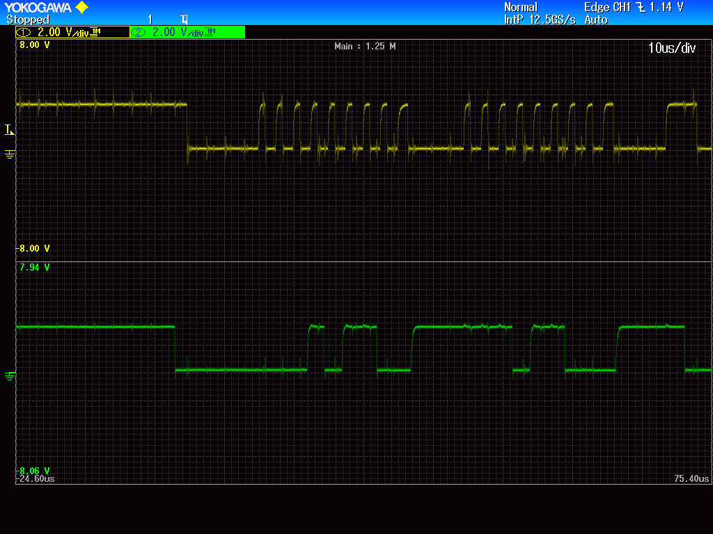
The result shows that we found an error message and it was not accessible.
We also found the evaluation circuit board itself has no problem.
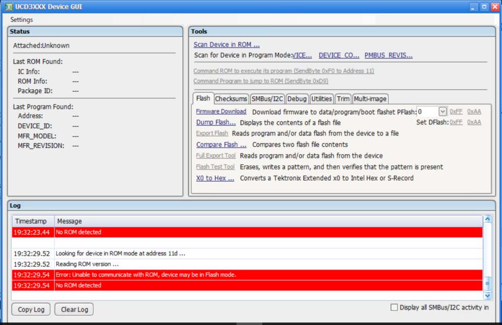
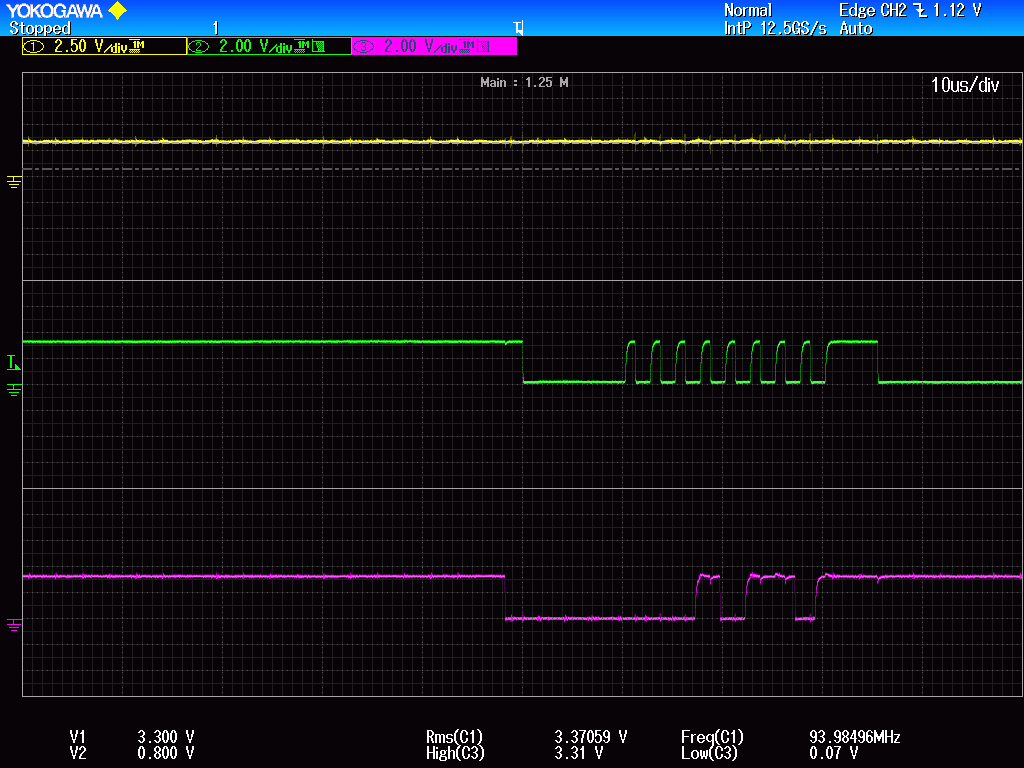
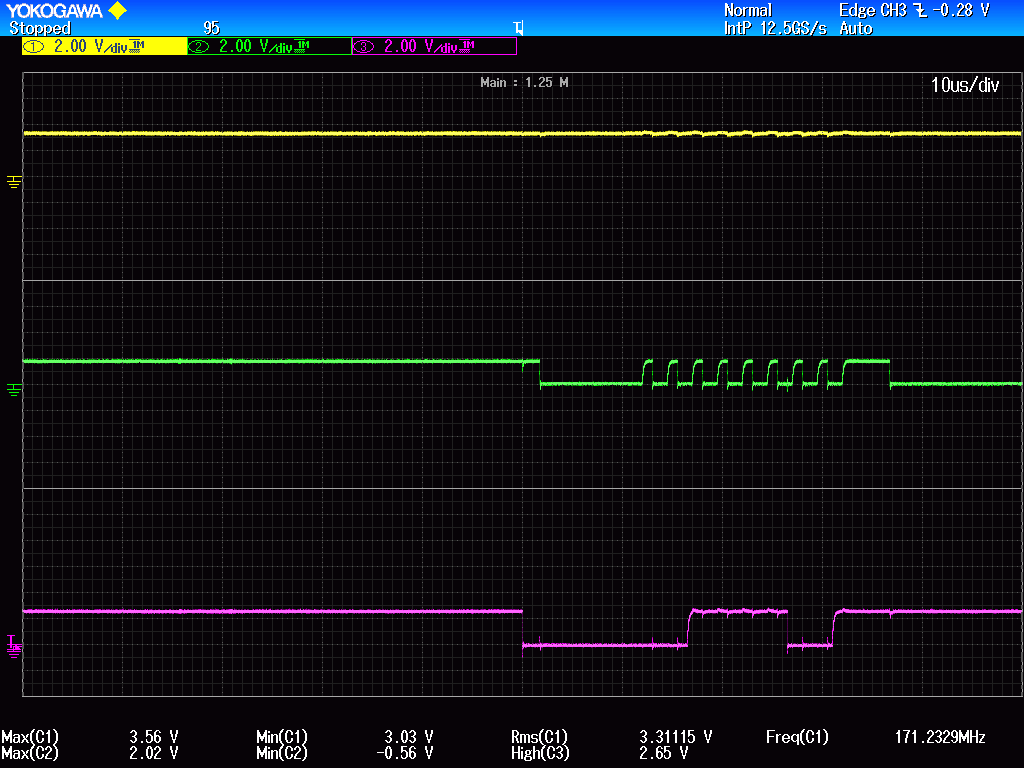
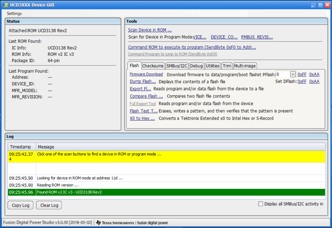
2.We checked our PC recognize the IC having using Fusion Digital Tool Launcher _UCD3XXX Device GUI and found it could recognize the IC when we executed Scan Device command.
3.We guess that it is because our PC cannot recognize the command Device _ID and SETUP_ID that we cannot access with Fusion Digital Power Designer.
We think we would access it if we write FW in the IC using Fusion Digital Power Production Tool but following error message showed up and it doesn’t work rightly.
Based on Script Writer, we make XML file and we operate in order of Load→Run Script and push start after Load Script read FW.Then we find the error message.ID setting might not goes well.
Dear Mr.Ian,
Thank you for your message.
We installed Fusion Digital Power Studio and tried scanning device. The same error message is displayed.
After installing UCD3xxx Design GUI, tried clicking on the Scan Device in ROM mode and the Device ID selections.
However an error message is displayed.
We have confirmed the green light comes on after plugging the USB to GPIO adapter into the PC first.
Using board was produced by us. We use PMbus interface for the first time.
We scoped the PMBus interface line and figures were displayed.
[CLK]
[DATA]
This UCD have not been programmed.Do we need to installing some program into the UCD?
best regards,
So this is your board, and this is the first time you have tried to do PMBus communication.
Since you have not downloaded a program to the chip yet, it should be in ROM mode. So you should be able to find it by looking for a device in ROM mode.
The first thing to check is if the chip has power to the proper pins. Please check all the power pins and ground pins to verify that they have the correct voltages on them. Verify that there are 1.8 volts on the BP18 pin.
Then put scope probes on the PMBUS_CLK and PMBUS_DATA pins and send the Scan Device in ROM command. If it works, it should look like this:
If the chip is not responding, it will look like this:
This is the first byte sent by the adapter, the address of the device in ROM mode. Yellow is PMBUS_CLK, blue is PMBUS_DATA. On the ninth clock high period, the UCD should ACK by pulling that PMBUS_DATA line low. If it does, the adapter continues to send and receive data. If it doesn't, the adapter will return an error. Please send a scope shot of the first byte sent on your system. Make sure to measure the signals on the actual device pins.
If you don't find anything else, try pulling the reset pin low after the chip is powered up. This will help if the power up sequence doesn't meet the spec.
If you can measure UCD current by itself, it should be around 60 to 80 milliamps, unless the DPWMS have significant loads on them. If you pull the reset pin low, you should see a drop of 10 to 20 milliamps. This can be useful even if you can't isolate the UCD in the system, you should still see the same drop in current.
Dear Mr.Bower,
Thank you for your reply.
We checked all the power pins and ground pins to verify that they have the correct voltages on them. 3.3 V was normally applied to the power supply pins and 1.8 V appeard on BP 18 pin.
We put scope probes on PMBUS_CLK(Yellow) and PMBUS_DATA(blue) pins and sent the Scan Device in ROM command. Then the following figure appeared.
This is the same as the waveform when the chip does not respond.
We pulled the reset pin low after the chip was powered up. But no change was observed. The current of UCD alone cannot be measured with the current setup.
best regards,
Thank you for your message.
Do we need to add UCD device to the script using Fusion Production tool.
best regards,
Yes that is correct. There are different devices in the UCD3xxx family that can be targeted for download so you'll need to configure the script accordingly.
However, until you can get the chip to respond to simple commands, the production GUI is not going to work.
It looks like you've got the right signals going to the clock and data pins. So if you've never programmed the chip, and it is connected correctly, it should respond.
There seems to be a problem somewhere on your connections to the chip. Maybe reset is pulled down all the time?
Another possibility is that you have a pin with a voltage above or below the supply rails?
Maybe pin 1 is in the wrong place? That's my personal number 1 mistake with socketed chips.
We reviewed the circuit and there is something that we are worried about.
When PMBus connector is connected and UCD power supply is low, 0.8 V is applied to reset pin. Is this a problem?
We think pin 1 is in the correct place. What do you think?
Even when RESET was Hi and Low, communication did not change the PMBus, and the clock when it was not responding was observed.
Yellow:RESET signal Green:CLK Red:DATA
[RESET HI]
[RESET LOW]
We have constituted the circuit like the evaluation model UCD3138PSFBEVM - 027. Does it work with this circuit?
Hello,
the partid will correspond to what you have in your firmware for the device id. So for UCD3138 regardless of pin package it will use UCD3100ISO1 .
If you look in your firmware code you will like find that in your device id string.
I can't see the symbolization on the chip, but actually, if you have 1.8 volts on BP18, that's a good indication that the chip is put in the right orientation relative to pin 1.
As far as the .8 volts on the reset pin goes, that is interesting. What is more interesting is that on your scope shot the reset pin doesn't look like it's all the way up to 3.3 volts, and it looks like it's noisy?
There was an issue with pulling up the PMBus pins and providing phantom power to a UCD that was not powered up, and it did cause the device to reset improperly. But I think a reset low and high would deal with the issue. The current version of the 3138 has the PMBus Clock and Data open loop to deal with this issue, but if you are pulling up ALERT or CONTROL, the problem could still occur.
The reset pin is very high impedance, You should be able to easily pull it down to ground and up to 3.3. I'd look there for your issue.
We put scope probes on ALERT(Yellow), PMBUS_CLK(Blue) and PMBUS_DATA(Red) pins and sent the Scan Device in ROM command. We also measured the CONTROL(Yellow), PMBUS_CLK pin (Green) PMBUS_DATA pin (Red) as well.
Yellow:ALERT Green:CLK Red:DATA
[TURN OFF]
[TURN ON]
Yellow:CONTROL Green:CLK Red:DATA
[TURN OFF]
[TURN ON]
We are concerned about noise when turning on the power
Can you see any abnormalities?
Also, please tell us the basic things.
We would like to know the procedure to use when purchasing IC (UCD 3138).
·Operating environment
· Connectors to be used (PMBUS, JTAG)
· Software to use
· Initial setting (Is it necessary to construct a script? How to set it?)
Reminder
Hello Mr.Ian,
Your immediate response is highly appreciated.
best regards.
Thank you for your response.
Currently we are investigating the problem again.
I found some points that are worrisome, so please let me know.
・What role does CONTROL play?
・What kind of waveform should CLK show when sending the scan device in ROM command?
・Process of entering ROM mode (since turning on the power)
・Relationship between resistance values of AD 00 and AD 01 and setting addresses
best regards,
Control doesn't plan any role, unless you have it pulled up before powering on the device, in which case it may cause the power on reset not to work.
The CLK waveform should meet the PMBus spec. If you use the USB Interface adapter with the correct GUI, and a good PMBus interface, you should get a good waverform. It looks like you've got a good one from the scope shots. I'm assuming that the glitches I see are just from not connecting grounds on scope probes. If they are actual glitches that go down lower than can be seen on the low res screen, then you may have a problem. Also, it looks like the levels are good enough, but you've got the scope voltage resolution set low as well, so I can't be sure.
When the UCD comes on, it configures some trim registers, and then reads the program flash, If there is a valid checksum, it will jump directly to the program and start executing. This is the most common reason for the programming to fail - there is a program already downloaded which doesn't respond to PMBus commands to clear the checksum. You say you haven't downloaded anything, so I've been not addressing that possibility.
If the checksum isn't valid, then it will go to ROM mode.
In ROM mode, there's no relationship between the resistance values on the AD pins and the address. The address is fixed.
Have you looked at the reset line? The level looked suspicious to me?
Thank you for your reply.
We reviewed the PMBus line and found that the resistance value of the DATA line was wrong.
We ran Scan Device in ROM mode using the UCD 3 X X X Design GUI.
The waveform at that time is below.
In this state, I started FUSION DIGITAL POWER STUDIO that I taught from past interactions.
However, the software was not activated by NO DEVICE FOUND.
The reset signal looks like the waveform below. Yellow: Power supply, Green: Reset signal
The high level is 3.3 V and the low level is 0.74 V.
If I can confirm that I can scan, will I be able to use FUSION DIGITAL POWER STUDIO as the next step?