This thread has been locked.

If you have a related question, please click the "Ask a related question" button in the top right corner. The newly created question will be automatically linked to this question.

UCC28070: UCC28070

Part Number: UCC28070
Other Parts Discussed in Thread: UCC27524, , UCC37324

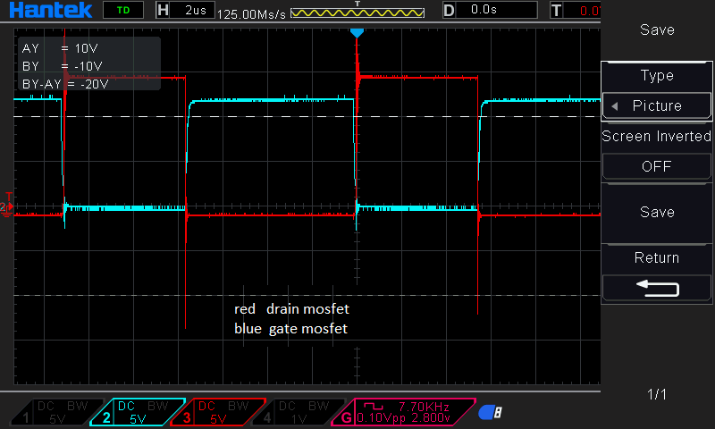
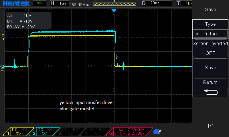
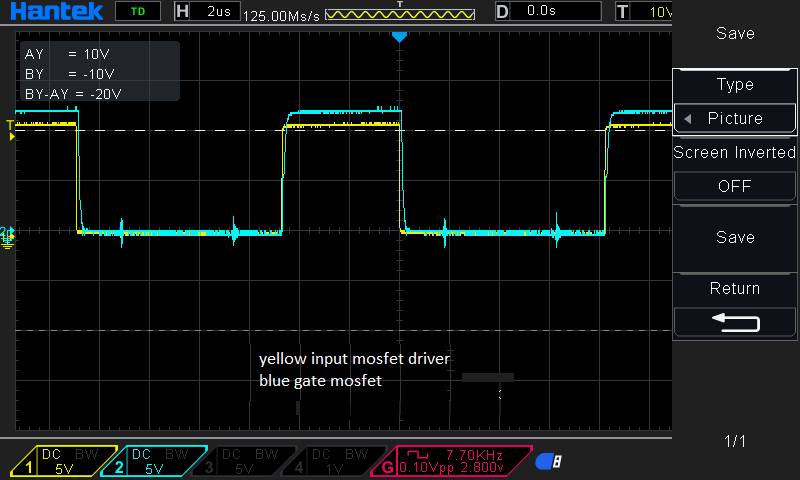
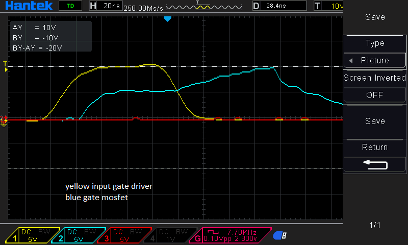
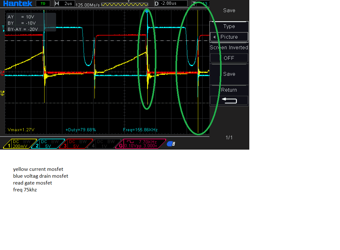
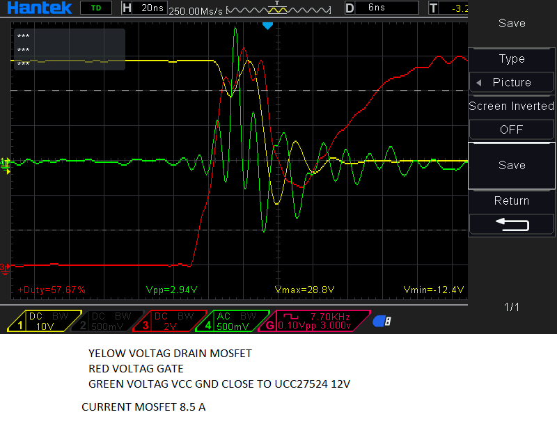
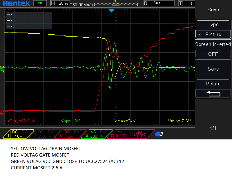
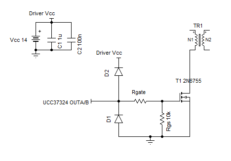
I TRY TO START WITH UCC28070 AND MOSFET DRIVER UCC27524 I HAVE PROBLEM AFTER CONNECT 220V UCC27524 IS DAMAGE SHORT OUTPUT PIN AFTER PUT ON FAST DIODE 1A UCC27524 WORK SOME TIME AFTER PUT LOAD FAST DIODE IS SHORT 

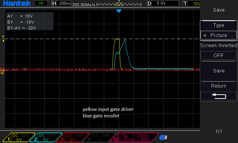
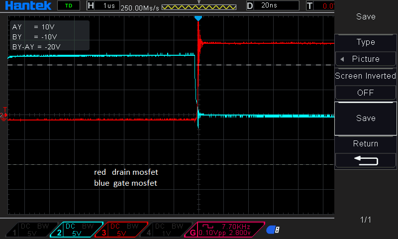
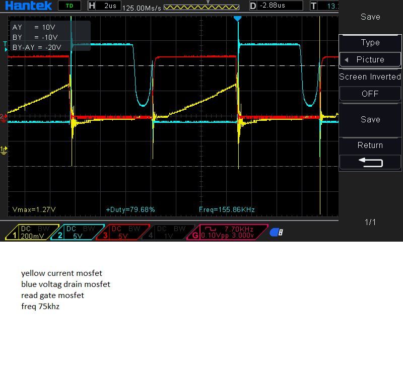
WHY MUST HAVE REVERS VOLTAG MORE THAN 1A ON GATE MOSFET ?

HOW CAN RESOLVED 

  • Hi Omid,

    Can you post your schematic so we can help solve your problem.

    Thanks

    Peter
  • hi yes I attach for you thanks 

    4kw.pdfCONTROL.pdfto you for 

  • Hi Omid,

    Thanks for posting the schematic. I think the issue concerns the UCC27524 and not the UCC28070 so I will ask the AE from the drivers team to help support your applications. In the meantime can you post oscilloscope images of the input and output signals of the UCC27524.

    Thanks

    Peter
  • Hi Omit,

    Sorry about your trouble and thank you for using our devices, my name is Mamadou Diallo from High power drivers group and I will help resolve your issue.

    If i am understand the issue correctly, when you're switching without the 220V bus connected, the driver operates correctly. When you connect the 220V bus, the driver fails immediately? and when you add the 1A fast diode, the driver works for some time before failing. Does that describe the issue you're experiencing?

    When you add the fast diode, how long does the driver operates correctly before failing? Please share any scope shots of the outputs OUTA and OUTB you may have captured.

    While you provide those clarifications, I will review schematics and get back to you as soon as possible.

    Thanks.

    Regards,

    -Mamadou
  • Hi Omid,

    I am going over your description again but still not clear on the failure description: is the UCC27524 device damaged (pin shorts or opens, for example -- is there any visible mechanical damage? heating, smoke,...)? Or is the output simply not following the input? Does the failure recover when you cycle the power to the system OFF and then ON?

    Do you have oscilloscope screenshots of what INA, INB, OUTA, OUTB, and VDD? These will be helpful for the debug process.

    Thanks in advance for the clarification.

    I look forward to hearing from you.

    Regards,

    -Mamadou
  • THANKS FOR YOUR HELP 

    1. I TRY FIRST 60V GET TEST ALL OK NO HAVE PROBLEM AND  2KW LOAD  OK WORKING

    2.AFTER CONNECT 220V FAILS IMMEDIATLY

    3.ADD DIODE 1A FAST DIODE GND AND OUTPUT GATE DRIVER  AND ONE 10K 0603 TO GATE MOSFET  AND GND

    SOME TIME 10K 0603 IS SHORT AFTER THIS CHANGE TO 10K 1206 NOW DIODE IS FAILS SOME TIME

    WILL BE TRY TO GET SOME CAPTURE FROM SCOP GATE AND SEND TO YOU  OK FOR YOU GET CAPTURE FROM 60V LINE POWER OR NEED 350V DC CONNECT AND GET CAPTURE FOR YOY 

  • NO HAVE ANY MECHANICAL DAMAGE AFTYER CHANGE FAST DIODE SOME TIME DRIVER WORK GOOD SOME TIME FAILS DRIVER MUST CHANG TO NEW ONE
  • Hi Omid,

    Thanks for getting back to me.
    Have you tried increasing your gate resistors? Also the R18 and R30 close enable pins are unnecessarily high, consider reducing these values as it could slow/delay the enable pins turn on.
    Also consider increasing your gate resistor which would decrease the switching times of the MOSFET and therefore reducing dv/dt and di/dt.
    Your gate capacitance at 127nC is pretty high. I wonder at what frequency you're switching these fets. higher the switching = higher power dissipation of the driver especially with small gate resistor. Please let me know at what frequency your switching as well
    When you provide the waveforms, please include those waveforms when the driver is working properly at 60V and all the relevant parameters to help debug process.

    From your schematic, beside the R30 and R18 being a bit high and maybe high gate charge if you're switching at high frequency, I do not see any particular issue that could've caused the failure. In your layout, I wonder if you made sure to minimize any loop inductances on the power stage.

    Thanks for the clarificattion and I look forward to hearing from you.

    Regards,

    -Mamadou
  •       phaseshift.pdfphaseshift-driver.pdfhi thanks for your follow my problem 

    r18 and r30 easy can change to 1k bout after connect power I have delay for start to switching pulse 

    I test with 60v again ucc27524 fails bout this time diode is ok when work no have any heat on ucc27524 

    frequency is 75khz 

    in other project I have problem phase shift switching power I attach for you all document wave picture 

    transformer 1:1:1 1.5mh in this case r13 r14 is heat and ucc27524 is heat bout working no any fails 

  • hi

    I think this is used full for you better can help to you 

    thanks 

  • hi
    new happened I try to 132v voltage out pfc test and send wave picture to you all is ok after this try out put voltage to 265 v again get test without load ok load 5.5A ok after try to load 10A ucc27524 one output short to vcc damage mosfet
    q6 and q6.1 is same load and one signal for driver why one is fails other is ok ?
  • Hi Omid,

    Thanks for sharing your waveforms.

    The waveform i attached below is likely due to coupling mismatch of secondary to primary winding which leads to excessive power dissipation that you observed on the driver and R13 and R14. Increasing your gate resistors could help resolve this issue.
    Note that you can determine this resistor value as follow: R >= 2*(L*C)^(1/2). Section 7.1 of this app note copied below discusses this matter in detail.
    www.ti.com/.../slua618.pdf

    Thanks

    -Regards,

    -Mamadou
  • Hi Omid,

    The MOSFET failure is likely due to excessive power dissipation at the junction terminals of the power FET due to simultaneous presence of high Ids current (yellow Ids) and high Vds voltage (Blue) for an extended period (longer than a quick surge). In your scope shots, it looks like Ids (yellow) never starts from ground. 

    It also seems like a lot of ringing on Ids current likely due to reverse recovery of the body diode. This excessive ringing could reach high values which in combination with Vds can damage the FET. Consider adding a diode very closed to FET in parallel with the snubber RC circuit you already have. 

    -One of the driver's output being also damaged leads to me suspect poor layout likely causing the stray inductance and capacitance. Minimizing the length of high current traces between the driver's output pins and the gate of the power switch is crucial.

    Please let us know if this resolves the issue by pressing the green button or reach out to us for further analysis.

    Thanks.

    Regards,

    -Mamadou

  •    HI

    I TEST DIODE NO CHANGE MORE ABOUT NEGATIVE VOLTAG

    I PUT 22UF CAPACITOR NEAR TO UCC27524 AND CHANG RC TO 20OHM 2.2NF

    I ATTACH PICTURE FOR YOU  

  •   HI

    I GET VOLTAG VCC AND GND CLOSE TO UCC27524 HAVE SOME RIPPLE ON DC VOLTAG WHEN SWICHING IS ON OR OFF AND WHEN INCREAS LOAD P-P VOLTAG IS INCREAS

  • Hi Omid,

    That is quite a bit of ringing going on. WHat you're experiencing is related to the effects of parasitic body diode reverse recovery on the mosfet (which is not optimized). It also explains the undershoot on the Vds and the noise on Vcc because the system is now susceptible to EMI noise. This is causing ringing on Vgs and losses with Vds and Ids overlapping (though you're not showing Ids).

    You're also switching too hard creating high dv/dt and di/dt. This large di/dt coupled with parasitic inductance in pcb layout will slow down switching transitions.
    Please increase gate resistance value (I noticed you only had Rgate = 5 ohm in schematic) to reduce dv/dt and di/dt, this will decrease turn on/off of the MOSFET.

    This should resolve the issue. If it does, please press the green button or let us know for further debug.

    Thanks

    Regards,

    -Mamadou
  • HI Mamadou

    i attach for you ti shematic for 3kw 

    no have rc on mosfet and gate 5.1 ohm only for remind you 

    i change R gate to 20 ohm and rc r=20ohm c=4.7N  still undershoot have bout lower than 5 ohm  

    again change 33 ohm undershoot around 20v bout temperature mosfet go up around 10 degree after this try test with low inductance when L/3 with 20 ohm good effect

    bout efficiency 5% down 

    under shoot 

    i think this problem searching on ucc28070  must select suitable duty on load when duty is high energy more save on inductor and make under shoot when mosfet turn on still inductor have current make switching hard   

    3kw.pdf 

  • Hi Omid,

    Sorry  you're still having trouble.

    I agree, ucc37324 is set up correctly, I don't see any issues related to the driver from the schematic shared.

    Before I pull the technical experts from ucc28070 team though, have you tried the configuration below?

    I know you already Rgs and Rgate there but the clamp diodes as shown might help with the gate malfunction.

    The gate going high before coming down just to go high again tells me something not right there.

    Also, I want to add a 0.1uF cap to help with the filtering. 

    If you're still having issues then, i would suspect UCC28070 and the duty cycle at full load.

    At that point, we will pull technical experts from ucc28070 team to help debug further.

    Thanks for your patience and perseverance. 

    Regards,

    -Mamadou

  • HI
    THANKS
    I WRITE FOR YOU BEFORE I ADD 10UF AND 0.1UF AGAIN (HAVE ONE SET ADD ANOTHER) TO VCC AND GND AFTER THIS EFECT SOME BETTER (WAVE VOLTAG EFECT GOOD BOUT NOT COMPLETED RESOULVED )AND NO FAILS UCC27524
    ABOUT D1 FIRST NO HAVE BOUT AFTER FAILS IN 220V I ADD D1 WITH HAND NOT SHOW IN SCHEMATIC AFTER CAN WORK WITHOUT LOAD ON 220V IN FUTHER ADD 1N4148 FOR D1 AND D2
    NOW MY PROBLEM IN HEVY LOAD SURE UCC27524 NOW SETUP CORRECT OTHER PROBLEM ON UCC28070 MUST FINED
    THANKS FOR YOUR BEST SUPPORT