This thread has been locked.

If you have a related question, please click the "Ask a related question" button in the top right corner. The newly created question will be automatically linked to this question.

UCC28950: UCC28950 SR FET rating selection question

Part Number: UCC28950

Hi All,

My name is Mert Karadeniz an electrical engineer works on Power Electronic Circuits in Germany.

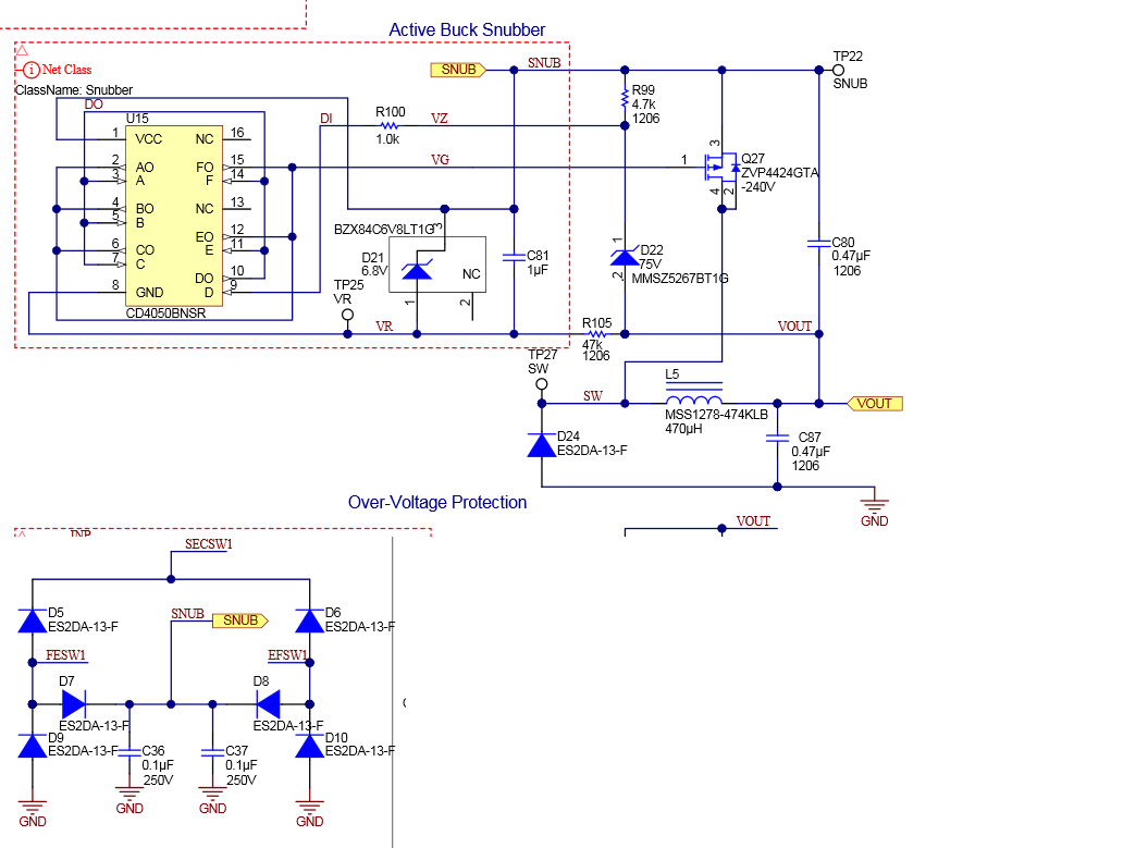
I have the same question of the operation principle of the circuit given above. Can someone briefly explain me how does the active snubber with hex buffer, P-MOSFET and zener diodes work?

Thank you very much.

Kind regards,

Mert.

  • Hello Mert.

    The circuit schematic doesn't appear in your post (this happens sometimes if you simply cut and paste a schematic rather than using the 'insert a file' button.

    Anyhow, please re-post the query so that we can keep the thread open and email me a copy at colingillmor@ti.com

    Regards
    Colin
  • Hi Colin,

    I have sent you the e-mail. Thanks a lot!

    Kind regards,

    Mert.
  • Hello Mert

    Thanks for sending me the email - I've replied directly to you but I'm updating this post as well

    From what I can see the CD4050 simply acts as a buffer and MOSFET driver which turns Q27 on when SNUB gets ‘too high’ and turns it off when SNUB gets ‘too low’. This action is hysteretic, controlled by the thresholds of the hex inverter alone. Q27 / D24 are the buck switching elements and L5 is the buck output inductor.

    C81/D21 give a regulated VCC rail for the hex buffer – actually it’s really a single non-inverting buffer because all the individual buffers are paralleled.

    R105 drops most of the voltage between VOUT and the cathode of D22 – the current is low of course.

    SNUB is a DC level regulated at about 130V by the Active Buck Snubber. The basic outline is in the attached document along with some waveforms.

    I’m afraid I haven’t actually seen this circuit before and I don’t have a PMP6712 device here to work with. I would have to run some simulations to give more details and that might take some time.

    At a top level. The snubber stores energy at about 130V in C73/C72/C36/C37 and the buck converter down converts this to VOUT – synchronously with the main power train.

    I’m not sure why the designer chose this method to control the buck active snubber but of course there are always different methods to achieve the same result.

    Please let me know if this answer is sufficient

    The full PMP6712 schematic is available at http://www.ti.com/lit/df/slura08/slura08.pdf

    Regards

    Colin