This thread has been locked.

If you have a related question, please click the "Ask a related question" button in the top right corner. The newly created question will be automatically linked to this question.

TPS22918: Usage of load switch output when the external input is applied

Part Number: TPS22918
Other Parts Discussed in Thread: TPS22917,

Hi Alek,

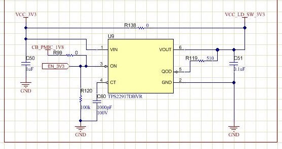
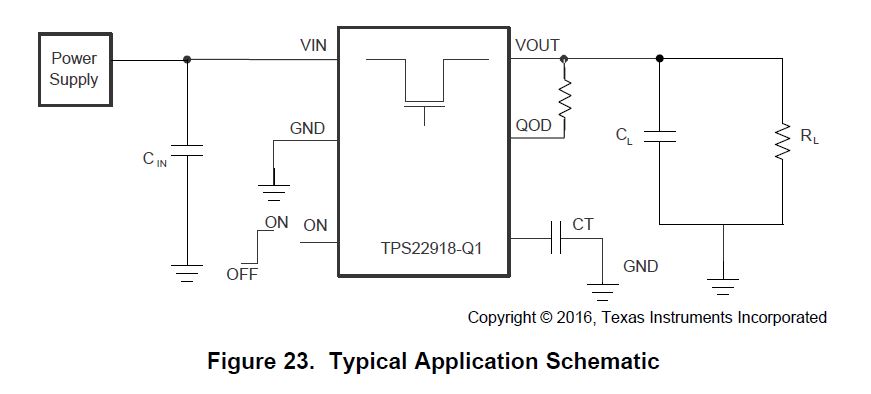
We have used TPS22917 IC as you have suggested which will add only reverse blocking protection compare to TPS22918 load switch. We are seeing difference for the CT pin as it is connected to GND in the TPS22918 datasheet and it is connected to VCC in the TPS22917 datasheet. We have used TPS22917 IC and connected to GND and please let me know what will happen if it is connected to GND. Please find the attached images for your reference.

Please let me know why CT circuit is different in both datasheets. 

Regards,

Sathyasai

  • Hi Sathyasai, 

    Thanks for reaching out on E2E! Alek has moved over the systems role in Power Switches. To introduce myself, I am the new Applications Engineer covering load switches, power mux, and low side switches.

    The TPS22918 uses an NFET for the internal pass FET, whereas the TPS22917 uses a PFET. Depending on which type of FET you choose, the device will turn on differently and Ct will impact the turn-on different:

    1. In the NFET architecture (TPS22918), we have CT connected to GND. In order for the NFET to work properly, the gate of the FET needs to be higher than the source of the FET (VOUT). In order to get Vgate higher than Vout, an internal charge pump charges Vgate. By introducing a CT capacitor connected from Vgate to GND, this slows down the charge time on Vgate.  
    2. In the PFET architecture (TPS22917), CT is connected to VIN. In order for the PFET to work properly, the gate of the FET needs to be lower than the source of the FET (VIN). At the start, the voltage on Vgate is the same as VIN. As the device turns on, Vgate is pulled to GND via an internal switch. By adding CT from VIN to Vgate, this slows down the pull-down time from the internal switch.

    Please let me know if you have any additional questions!

    Thanks,

    Arthur Huang


  • Hi Arthur,

    Thanks.

    We have used TPS22917 and connected CT pin to GND instead of VIN in our design. Will it create any problem.

    Please find the attached schematic for your reference.

    Regards,

    Sathyasai

  • Hi Sathyasai, 

    Yes, this will cause additional stress on the internal channels used in the CT connection. At lower CT values it won't stress the device as much, but in either case we recommend that the CT pin not be connected to GND on the TPS22917. 

    Thanks,

    Arthur Huang

  • Hi Arthur,

    Thanks for the explanation.
    As you mentioned, By adding CT from VIN to Vgate, this slows down the pull-down time from the internal switch in TPS22917. As we already received the assembled board,I will remove the capacitor(C60) in our design. Please let me know the impact if the capacitor is not connected from VIN to Vgate. Will it reduce the time delay from VIN to VOUT?

    Regards,
    Sathyasai
  • Hi Sathyasai, 

    Without the CT capacitor connected from VIN to the CT pin, the device will ramp up with the fastest timing. The speed that it ramps up will ultimately depend on your output load and VIN, you can approximate the turn on time from page 6 in the datasheet, or run the tests on your board for more accurate results.

    Thanks, 

    Arthur Huang

  • Hi Arthur,

    As per the datasheet turn on time is 120us(3.3V) which is fine for us.
    Thanks for support.

    Regards,
    Sathyasai