This thread has been locked.

If you have a related question, please click the "Ask a related question" button in the top right corner. The newly created question will be automatically linked to this question.

TPS2546: What will happen if no D+/D- communication is completed before drawing current from Vbus?

Part Number: TPS2546

Hi Chuck,

       The last question went way too long so here I begin a new one with more specific question.

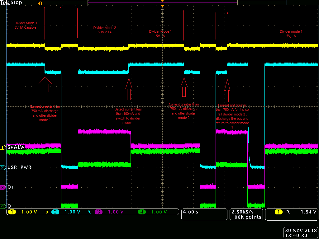
       In the case that CTL1, CTL2, CTL3, ILIM_SEL is set to 0111 for S5, and directly drawing 2.1A current from Vbus without D+/D- communication, are the discharges happens in the attached waveforms normal? Could you help to explain the reasons?

       Thanks very much for your support.

1

  • Max,

    I do not have enough resolution in this capture to say for sure, but it appears that the load is applied and this causes the load detect feature to be engaged which causes the first discharge. The load is then removed before the discharge delay has expired which causes a second discharge.

    After this second discharge completes, there is a 15s timeout before the process starts again.

    Is your customer able to spread out the time between changes in load to about 8x what is shown in this figure and then tighten them until this behavior happens again? This will allow me to better see what is happening.
  • Chuck,

    I attach the two scaled-up waveforms as follows(both under S5: 0111). They are captured by scope so I'm afraid it is the best resolution we can provide so I suggest you to save the pictures and scale up to see the detailed divisions by softwares if it still seems not clear for you. 

    And here again note that the D+D- is not connected, we can currently focus on the light blue(marked "USB_PWR" waveform) which are Vbus waveforms. The time scale for both figures are 4s/div.

    Take the first waveforms below as an example, the first discharge takes place after drawing 2.1A from Vbus for about 2s and then the first discharge for is caused by load detection feature right? And the discharge takes the whole 2s delay before Vbus is pulled up. And then after released for 1.5s the discharger happens again. I get confused because I found that Vbus is not discharged after a longer loading time after release in the 2nd capture. Is this normal? 

    For the 15s timeout, why shall we start from the 2nd discharge? Could you explain more detailed please?

    Are the two waveforms below enough to reach an conclusion for these discharges? Since it has been twice that we contact the customer for more test and feedbacks before, I think it is better that we can draw an conclusion in this round if we need the customer to arrange more test. So could you list in detail of the waveforms you need for judgement please?

    Thanks for your help.

    2

  • This diagram shows the device is pulling D- and D+ to ground which causes the first bus discharge and begins the primary and secondary detection.


    It appears that the device fails secondary detection because D- is not driven to 2.7V and this causes a discharge and redetection which attempts to enter 1.2V mode and fails and the device then enters SDP mode and yields control of D+/D- to the device.

    Is the downstream device a SDP only device?

    Regards,
    Chuck
  • Chuck,

    Seems we have some misunderstanding on the test condition. Please check the following block diagram. The customer directly drawing current by a electronic load on Vbus and D+/D- are not connected. So the test is not finished with a device but only with an electronic load thus no detection on D+D- are done and we directly loading on Vbus. How will this influence the behavior of TPS2546?

    Based on this test condition, can you help to explain the reason for each discharge shown in previous two waveforms.

    Thanks for your help.

    3

  • Max,

    Does this pattern repeat over and over again?

    In DCP mode, there are specific voltages and connections required of the downstream device. None of these are met in the condition where D+/D- are not connected and the part will cycle through it's entire detection scheme over and over. This is what you are seeing on your capture.

    A simple test to prove this is to short D+ to D- with a resistance less than 200 ohms for this test. This will force the TPS2546 into DCP shorted mode and will provide the target 2.1A of current.
  • Max,

    Let me also explain each change in the diagram with more detailed text:

    1. The part starts off in divider mode 1 (5V, 1A) with a current limit of ILIM_MAX which is greater than 2.1A in this case.
    2. The part detects that the current draw is greater than 750mA and performs a discharge and then presents divider mode 2 (5.1V, 2.1A) The part will test to see that the current draw remains greater than 750mA for more than 4s and will stay in divider mode 2.
    3. The current changes from 2.1A to ~0A. The part detects this current change and switches back to divider mode 1 without a discharge to not disturb the phone. It will remain in this mode indefinitely.
    4. This is the second application of 2.1A. The part detects this change and repeats the steps in #2. It discharges the bus and offers divider mode 2. In the second instance, the current is reduced before the divider mode 2 detection is complete, so the part discharges the bus and returns to divider mode 1.

    Please let me know if this resolves your question or if you need further support.
  • Hi Chuck,
    Thanks so much for your detailed reply. Just one more question. Is the 4s here claimed by datasheet or follow some specs? Or it is an estimated value based on some settings?
  • Max,

    The 4s is build into the design and will be as consistent as the other timing specifications, but is not part of the datasheet.

    Please click customer thinks resolved if I have fully answered your questions.