Because of the holidays, TI E2E™ design support forum responses will be delayed from Dec. 25 through Jan. 2. Thank you for your patience.

This thread has been locked.

If you have a related question, please click the "Ask a related question" button in the top right corner. The newly created question will be automatically linked to this question.

UCC27714: Dead band residue

Guru 54778 points
Part Number: UCC27714
Other Parts Discussed in Thread: TIDA-00778,

Hello,

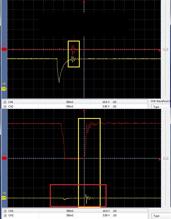
Please help determine why synchronous dead band delay (80ns) HO falling, LO rising edges seem to cause LO ringing along ground (-5-10v) during HO fall/rise pulses. When dead band immediate update, LO falling/rising edges cause HO ring residue pulses during LO low pulse times.  Overlapping PWM signals on HI/LI inputs drive the HO/LO outputs produce dead band delay only for last PWM cycles Ton NFETS. The last on NFETS exist across two of three UCC, one high side one low side. 

Perhaps internal creepage or indirectly HI/LI cause dead band delay residue on opposite outputs?  Could HI/LI input filter (200pf/51ohm) be causing cross talk on AGND that LO picks up via COM? 

How can HO/LO dead band residue ringing pulses be mitigated?

  • Hello BP101,
    Without seeing the scope waveforms I can comment on what may be the cause of the ringing you mention, but I am limited on understanding the details.
    It sounds like in a case of 80ns dead time of HO and LO you are seeing excessive ringing relative to ground. One source of ringing during switching is the switching edge dV/dt which can generate ringing due to energy transfer in parasitic capacitance, and also dI/dt can generate a voltage potential in parasitic inductance, typically of the board traces. The turn on and turn off of the Mosfet gates involve driver peak currents to charge and discharge the MOSFETs, this peak current does flow into the source terminal and can generate ring in the trace parasitic inductances.
    If the drain to source Vds fall/rise times and other Mosfet gate drive align when both are generating voltage spikes and ringing, it makes sense that certain switching dead bands could generate higher ringing in the ground paths.

    It is not clear if you are saying there is differences in driver delays in these conditions. It is possible with varying peaks or ringing on the driver input signals into the filter with result in a different delay from the filter. Specifically a higher voltage peak into the filter will result in less time to reach the driver threshold voltage. I see that the filter is only ~10ns, so my initial thought is that this possible variance in signal into the filter should not cause significant delay differences in the filter.

    Internal to the driver, since there is no logic limiting LO and HO independent operation there should not be impact of dead time variance from one channel to the other.

    Ringing on LO and HO in general can be reduces by ensuring the gate drive current loop is short without high parasitic inductance. Also gate drive resistance will serve to lower the Q of the parasitic inductance and capacitance that exists in the gate drive output loop.

    Regards
    Richard Herring
  • Hi Richard,

    The point of post was to question how competition gate driver does not have this issue of dead band residue. Again dead band is not persistently enabled, delay is only added to HI/LI during GToff. It seems the UCC has some kind of timing issue, perhaps is not so compatible with overlapping HI/LI PWM signals? Seemingly timing/filtering issues must be clarified by TI engineering as being acceptable for overlapping PWM conditions where duty cycle PW on LO differs from HO PW. Note 1st capture LO 80ns delay effects HO at the very same time and HI dead band is not enabled at this time as HO is high. Ringing HO appears to be cross talk? Note 2nd capture LO is being effected by HO the exact opposite condition is not dead band time either. Yet ringing changes to opposite HO/LO relative to dead band being immediate update versus synchronous update. It seems to me TI is not aware of these issues of UCC drive being Space Vector PWM (TIDA-00778) controls HI/LI via unvaried duty cycles presented on HO/LO, reference SPRA-524.

    Randomly Synchronously adding 80ns delay to HI/LI should not impact the UCC as it seems to in capture, correct? The UCC gate loop is even shorter than competitions inverter PCB. Perhaps HI/LI timing is impacted by components choice, VDD bias or HI/LI inputs filtering. We saw very odd behavior competitions driver, 200pf added HI/LI via series 100 ohms. However 100 ohms alone gained some isolation from NFET dv/dt and never caused dead band GND residue or large voltage peaks on drain shooting into B+ plaguing inverter output MCU drive.

  • Hi BP101,

    Richard is on holiday. Thanks for posting your schematic, he will look at it and get back to you by Jan 4th.
  • Hello to all & happy new year,

    Still struggling to figure out why LO is ringing -10v below ground or if even related to dead band. It seems +15 VDD bias supply current changes during rapid HO rise/fall edges as HO seems to source reverse current from LO via COM and not VDD bias. All three UCC have the same issue. The negative LO pulses are unexplained switching artifacts from overlapping HI/LI signals, perhaps crossing just above 100ns minimum PW cut off threshold in duty cycle changes.

    Question remains how phantom residual LO pulses (yellow ovals) are being produced coincident with HO edge activity.

  • Hello BP101,
    Thank you for the detail on the scope plots, I will comment on likely causes of transients seen on the scope plots.
    Ideally, if we could see the HO LO and SW node on the same plot I could determine with more certainty the cause of the spikes on LO.
    A first couple of observations, the LO signal probe must be connected to traces that are some distance from the IC pins. The driver has internal high side and low side FET's which have body diodes to COM (pull down FET) and VDD (pull up FET). At the IC pins, the voltage would be clamped to lower voltage levels, similar to a diode drop, but higher Vf. The negative spike durations look fairly narrow which means there will not be excessive time for current to build in the internal FET body diode.
    Without seeing the SW node waveform, I will comment on what we see in most applications to some degree.
    HO turn off: when HO turns off the expected HS will transition from high to ground within the Vds fall time. The low side MOSFET Cdg capacitance (miller capacitance) couples charge into the low side gate resulting in generating a negative voltage during the Vds falling time.
    HO turn on: this one is a little more open to some speculation about what HS voltage is doing. During the HO turn on, and the expected HS rising time, the same miller capacitance has to be charged which will tend to generate a positive voltage, which you do see in the beginning. Any ringing on the HS voltage will be couple by the Cdg, which can explain the negative spike.
    If there is the opportunity to confirm what HS waveform looks like, compared to LO and HO, with similar plot scaling that will be helpful.

    Regards,
    Richard Herring
  • Hi Richard,

    These HO/LO captures are the SW node gate leg and do not cause similar H0/LO mirror pulses on competitions gate driver. Only recently discovered reading again TIDA-00778 that COM pin is provided for NFET drain lead to bypass shunt resistor inflicting ground noise. That statement is no where listed in the UCC27714 gate drive datasheet and we did not make the bypass NFET drain ground direct to COM. Recall past 200pf with 100 ohm HI/LI filters on competitions driver HO/LO were both very noisy and motor sounded terrible during acceleration. Removed all the HI/LI filter caps thus stopped odd harmonics from developing on HO/LO, wonder this case perhaps 100pf filters produce less ground bounce residue of HO? The odd part is dead band timing seems to effect what side the residue pulse (mirroring) end up on HO or LO.

    It seems LO phantom pulses being near ground are mirrors of HO drive path as COM is also shared in the HO level translator drive path. That may explain why we see phantom mirror pulse on COM side when ever HO fires and to much feed back occurs from the HI/LI input filter caps?

    Richard Herring said:
    If there is the opportunity to confirm what HS waveform looks like, compared to LO and HO, with similar plot scaling that will be helpful.

  • Hello BP101,
    The last suggestion you made regarding the level shifter for the HO being a possible contributor of the voltage transients on the LO signal, is not very likely. The pulse current to operated the level shifter is in the mA range of ~6mA. The perturbations you are showing will take considerably more current into a circuit with 50 to 130 Ohms resistance. Base on recent feedback on one of your other posts I am assuming the turn on resistance is 130 Ohms and turn off resistance is ~50 Ohms.
    In most cases, the induced voltage on gate drive outputs are a result of the miller capacitance charge/discharge during Vds dV/dt, as I mentioned in the previous post.
    It will be helpful to see the switch node waveform, compared to the LO perturbations you have illustrated.
    Is there significant parasitic capacitance on the motor windings which may help clarify the influence of HO gate drive current onto the low side FET gate?

    Regards,
    Richard Herring
  • Hi Richard,

    Richard Herring said:
    The perturbations you are showing will take considerably more current into a circuit with 50 to 130 Ohms resistance

    I was referring to the AGND (COM) feed back loop created by adding filter caps on HI/LI inputs. Ceramic capacitors block DC yet pass higher potential pulsing DC (dv/dt). To me It appears the HO driven NFET Qrr (dv/dt) recovery is leaking back to LO either via LI or the internal shared COM connection of level translator. Such excessive dv/dt (-10v) was never present with competitions driver, nor did overshooting B+ ever present >5v above supply, 24v-160v. Yet UCC HO/LO are not overshooting as defined by datasheet as exceeding VDD, +17v.

    Perhaps one way Qrr from HO driven NFET can perturbate into LO is via COM ground. The other is B+ yet LO eventually shoots >-10v, response to HO driven Qrr. I don't think you are correct in believing HO driven NFET Coss inflicts LO Ciss. Seemingly scope capture suggests internal creepage or cross talk HI/LI is occurring. Again how on earth is HO Qrr (dv/dt) getting into LO other than via creepage or HI/LI cross talk? The gate region of N channel FET is more hole reactive to removal of electrons so it should remain off as it mostly does, not always. Seemingly the HO Qrr condition on LO is being exacerbated by incorrect signal conditioning on LI/HI as used in TIDA-00778 and UCC datasheet. Seemingly HI/LI input filters lead to Qrr cross talk on HO/LO outputs via COM path.  

    Competitions inverter NFET Ciss=4600pf, Coss=400pf had virtually no spikes on B+. However same LO pulses mostly show above GND and never under shoot > -1v. The odd part UCC drive LO is not being commanded by MCU to turn on yet we see LO peaks near +5v well above VGS(th) 3v Min, 4v Typ, 5v Max. Dead band injects equal periods (HI/LI) and occurs as HO turns off but not as HO turns on, dead band delay is only 80-120ns. Competitions driver has much slower HO to Miller rise time, 5-10us arrests most all ringing at VDD peak.  

    Richard Herring said:
    It will be helpful to see the switch node waveform, compared to the LO perturbations you have illustrated

    There is NO real discernible difference in the shape of HO signal versus drain source inductive junction, in either case the same -10v pulses are present in the inverter output wave form at the very same place.

  • Hi Richard,

    Below are captures from competitions gate driver Infineon HEXFET Qrr (640nC Max) and UCC OPTIMOS-FD Qrr (640nC Typ) above post captures. One notable difference is LO side Qrr (dv/dt) seems much faster, HO peaks no ring. Notice HO is much faster turn on (5-10us) without 200pf filter caps, 100R series HI/LI.  Contrast UCC HO/LO with 200pf/51R filters (HI/LI) takes >.35µs to turn on NFET, ringing over peaks -10v dv/dt being left in the disturbance wake of Qrr.

    It really seems from this contrasting and rolling off gate turn on time via HI/LI 200pf filters are causing excessive Qrr mayhem with UCC driver. Might TI engineering verify slower Gton roll off can be destructive in this case >.35µs VGS full on.  Note too TI scope captures TIDA-00778 (Fig.37/41) HO rise 90ns, <1.6µs to full VGS on with the same 200pf HI/LI filters. UCC our case OPTIMOS-FD a much slower PWM slew rate 8ma drive current from MCU,  >.35µs VGS rise time.

  • Hi Richard,

    It would seem you have described a 3rd current path which is stressing HS junction via LO side, least dv/dt shows up there. That requires a technical brief describing best way to mitigate 3rd current path HS to internal UCC COM pin connection. Obviously floating HO side dv/dt seeks the least resistive path internally via HS to COM.

    Seemingly the drop of low side NFET body diode via shunt to ground is much greater than to internal COM tied directly to AGND. Again UCC datasheet fails to clarify either schematically or otherwise the LO side COM pin is best connected above shunt ground. TIDA-00778 only suggests COM pin tied to shunt mitigates ground noise, no mention of dv/dt or HS-COM internal 3rd current path develops. Seemingly that is why HO-HS dv/dt is also captured on LO output seeking 3rd COM path to ground via low side shunt. HS dv/dt 3rd current path must be slowed down or HS pin is being stressed.