


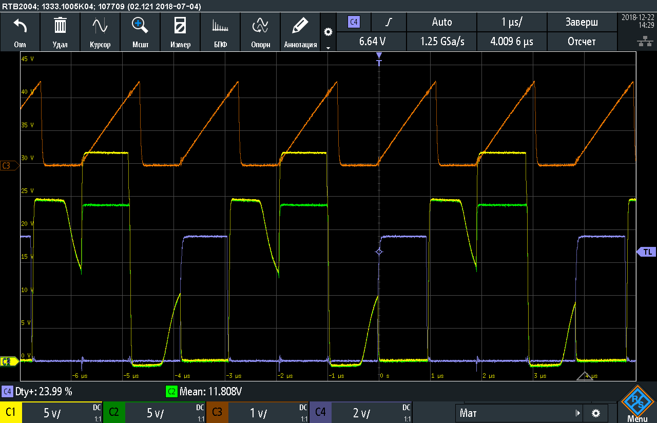
Orange - RAMP
yellow - HO
blue - LO
COMP=360 uA
CS=0 (closed pin IC )
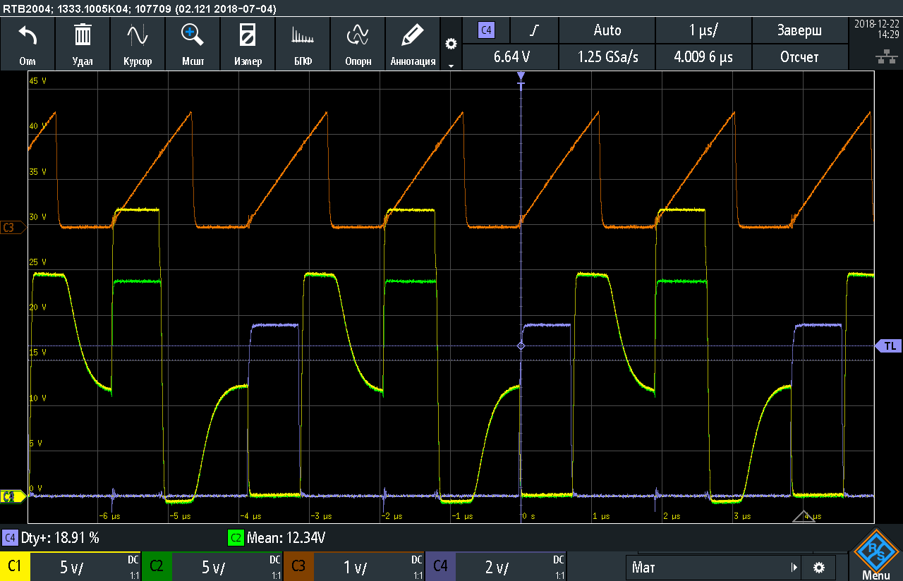
COMP=460 uA
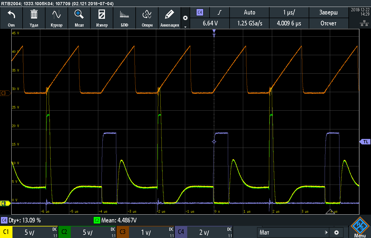
COMP=560 uA
in all examples, the transformer windings are loaded on resistors without rectifiers and capacitors
when the feedback signal changes (from 560 to 360 μA back), PWM does not restore symmetry to some value of the feedback signal (hysteresis)
